Base Clock Resources for FlexRIO Modular I/O FPGA Modules
- Updated2025-01-23
- 3 minute(s) read
Base Clock Resources for FlexRIO Modular I/O FPGA Modules
A base clock is a digital signal existing in hardware that you can use as a clock for an FPGA application.
Your FlexRIO with Modular I/O FPGA Module provides several base clock resources that can be used to run a LabVIEW FPGA VI. Use the table below to determine which base clock resources are available for your FlexRIO FPGA Module.
| Base Clock | FPGA Module |
|---|---|
| 40 MHz Onboard Clock | all FlexRIO Modular I/O FPGA Modules |
| PXI_CLK10 | all FlexRIO Modular I/O FPGA Modules |
| 100 MHz Clock | all FlexRIO Modular I/O FPGA Modules |
| 200 MHz Clock | all FlexRIO Modular I/O FPGA Modules |
| IO Module Clock 0/IO Module Clock 1 | PXI-795x, PXIe-796x |
| PXIe_DStarA | PXIe-796x, PXIe-797x |
| DRAM Clock | PXIe-797x |
Routing Diagram for
PXI-795x Base Clocks
On PXI-795x modules, the 40 MHz onboard clock is generated using a PLL outside of the FPGA. The 100 MHz clock and 200 MHz clock are generated within the device FPGA using a PLL.

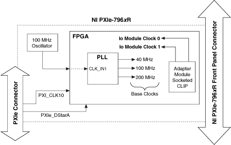
Routing Diagram for
PXIe-796x Base Clocks
On PXIe-796x modules, the 40 MHz onboard clock, the 100 MHz clock, and the 200 MHz clock are generated within the device FPGA using a PLL. The PLL source is the onboard 100 MHz oscillator clock. After the VI is downloaded, the FPGA detects whether or not the backplane 100 MHz oscillator clock is present, and if so, it configures the PLL to lock to the backplane 100 MHz oscillator clock.
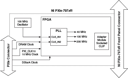
Routing Diagram for
PXIe-797x Base Clocks
On PXIe-797x modules, the 40 MHz onboard clock, the 100 MHz clock, and the 200 MHz clock are generated within the device FPGA using a PLL. The PLL source is either the PXI Express Clk100 backplane clock or the onboard 100 MHz oscillator clock. After the VI is downloaded, the FPGA detects whether or not the backplane PXI Express 100 MHz clock is present, and if so, it configures the PLL to lock to the backplane PXI Express 100 MHz clock. If the PXI Express backplane clock is not present (for example, in a CompactPCI Express chassis), then the device FPGA sets the PLL to lock to the onboard 100 MHz oscillator clock.