Specifications Explained: NI Multifunction Reconfigurable I/O (R Series)
Overview
Contents
- Introduction
- Understanding Specification Terminology
- Analog Subsystem Specifications
- Digital Subsystem Specifications
- External Clock
- Other Specifications/Terminology
- Additional Resources
Introduction
This guide is broken up into the same sections as most NI specifications manuals. Terms and definitions below are listed in a similar order to how the specification sheets are formatted. This guide exclusively applies to 78xx Multifunction Reconfigurable I/O devices and modules (formally known as R Series NI-78xx). Other NI product families such as cDAQ and cRIO Chassis and Controllers, 91xx, 92xx, 94xx C Series Modules, Multifunction I/O (MIO), Digital Multimeters, Scopes/Digitizers and other instruments may use different terminology or methods to derive specifications and as such, this guide should not be used as a reference for devices and modules other than those in the Multifunction Reconfigurable I/O (R Series) family.
This guide will use the PXIe-7847 device as references throughout. If you'd like to follow along with this device specifications, you can do so by following this link: PXIe-7847
Understanding Specification Terminology
First, it is important to note the categorical difference between various specifications. NI defines the capabilities and performance of its Test & Measurement instruments as either Specifications, Typical Specifications, and Characteristic or Supplemental Specifications. See your devices' specifications manual for more details on which specifications are warranted or typical.
- Specifications characterize the warranted performance of the instrument within the recommended calibration interval and under the stated operating conditions.
- Typical Specifications are specifications met by the majority of the instruments within the recommended calibration interval and under the stated operating conditions. Typical specifications are not warranted.
- Characteristic or Supplemental Specifications describe basic functions and attributes of the instrument established by design or during development and not evaluated during Verification or Adjustment. They provide information that is relevant for the adequate use of the instrument that is not included in the previous definitions.
Analog Subsystem Specifications
NI Multifunction Reconfigurable I/O (R Series) devices and modules may have analog input, analog output, or a mix of both systems. There are specifications unique to each subsystem, but also some specifications which apply to both. This section is organized in three sections to cover the common specifications, analog input specific, and analog output specific.
Analog Input and Analog Output
Absolute Accuracy at Full Scale
Accuracy refers to how close to the correct value of a measurement is. Absolute Accuracy at Full Scale is a calculated theoretical accuracy assuming the value being measured is the maximum voltage supported in a given range. The accuracy of a measurement will change as the measurement changes, so to be able to make a comparison between devices, the accuracy at full scale is used. Note that absolute accuracy at full scale makes assumptions about environment variables, such as 25 °C operating temperature, that may be different in practice.
- Residual Gain Error—Gain error inherent to the instrumentation amplifier and is known to exist after a self-calibration
- Gain Tempco—The temperature coefficient that describes how temperature impacts the gain of the amplifier compared to the temperature at last self-calibration
- Reference Tempco—The temperature coefficient that describes how accurate a measurement is at a specific temperature compared to the temperature at last external calibration
- Residual Offset Error—Offset error inherent to the instrumentation amplifier and is known to exist after a self-calibration
- Offset Tempco—The temperature coefficient that describes how temperature affects the offset in an ADC conversion compared to the temperature at last self-calibration
- INL Error (relative accuracy resolution)—The maximum deviation from the voltage output of an ADC to the ideal output. Can be thought of as worst case DNL. See also: DNL
- Random/System Noise—Additional system noise generated by the analog front end, measured by grounding the input channel
Example
The NI PXIe-7847R has a range of ± 10 V. The absolute accuracy at full scale (calibrated) is calculated with the assumption that the signal being measured is 10 V. The absolute accuracy at full scale for the ± 10 V range is 2,283 µV.
See Also
How Do I Calculate Absolute Accuracy Or System Accuracy?
Resolution
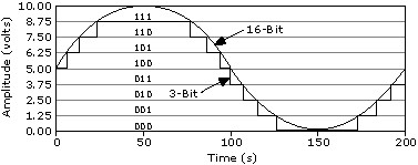
Resolution is the smallest amount of input signal change that a device or sensor can detect. The number of bits used to represent an analog signal determines the resolution of the ADC.
Example
The NI PXIe-7847R is a 16-bit device, which means that lowest amplitude change that can be detected on the ±5 V range is 0.152 mV. On the ± 1 V range, this value is 30.5 µV.
Range (Input or Output)
For analog input, this is the maximum positive and negative value that can be measured with guaranteed accuracy. For analog output, this is the maximum positive or negative value that can be generated. Some devices have multiple input or output ranges that can be used to provide a higher resolution at lower level signals.
Example
The NI PXIe-7847R as input signal ranges of ±1, ±2, ±5, and ±10 V. While the analog output range is ±10 V.
Coupling (Input and Output)
A property of the interface of two circuits that defines which types of signals are passed from one side of the interface to the other. There are generally two options:
- DC coupling: will pass both AC and DC signals
- AC coupling: will pass only AC signals, resulting in a hardware implementation of removing a signal's DC offset
Some devices feature software-selectable coupling, while some have either AC or DC.
Example
The NI PXIe-7847R has DC coupling on both the analog input and analog output. It does not support AC coupling on either.
See Also
Basic Information about AC and DC Coupling
Differential Non-Linearity (DNL)
The difference between the ideal step size of an ADC or DAC and the actual value that is input/output respectively (typically measured in LSB). In an ideal ADC or DAC, Differential non-linearity would be 0 LSB.
Example
The NI PXIe-7847R has a DNL of ±0.9 LSB maximum, which means that for any value that is input into the ADC, the actual value can be ±0.9 LSB away from the value read. For example, if the user reads the input of the ADC to be a value of 1 V on the ±5 V range, the input (not including effects of accuracy) can range from:
INL is the compound effect of DNL so the INL specification is often used in accuracy calculations. For the NI PXIe-7847R, the INL specification in the AI accuracy table is 42.52 ppm on the ±10 V
Analog Input
Analog-to-Digital Converter (ADC) Type
Successive Approximation register (SAR) is a type of ADC which implements a binary search algorithm to convert a continuous analog signal to a discrete digital representation.
Example
The NI PXIe-7847R uses a SAR ADC
Conversion Time
Amount of time that the input signal must be held constant while the SAR ADC performs the conversion. This is often done through sample and hold circuitry internal to the ADC.
Maximum Sampling Rate (per channel)
The fastest data acquisition rate that the PCI/PCIe, PXI/PXIe, or USB can achieve per channel.
Example
The PXIe-7847R has a maximum sampling rate (per channel) of 500kS/s. All R Series boards are simultaneously sampling (ie. Sampling rate per channel).
Input Impedance
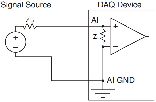
Input impedance is a measure of how the input circuitry impedes current from flowing through to analog input ground. For an ideal ADC, this value should be infinite—meaning no current will flow from the input to ground—but in practice this is not possible. The implication of some finite input impedance is that the ADC will have some degree of loading down a circuit, particularly those of high output impedance. It is typical for sensors to have low output impedance.
Example
The NI PXIe-7847R has an input impedance of Zin > 1.25 G Ω in parallel with a 2 pF capacitor. Taking the worst case scenario of lowest input impedance, you can view a single-ended measurement as the following simplified circuit, assuming a sensor with output impedance Zout = 150 Ω.
The series combination of the sensor output and DAQ device input means that voltage will be divided between the two impedance values, with the larger impedance bearing most of the voltage. This means that if the sensitivity of this sensor is 20 °C / V and is measuring 100 °C (outputting 5 V), then the voltage measured by the DAQ device will be the output voltage multiplied by the ratio of the input impedance to the sum of the DAQ input and sensor output impedance:
This .6 mV measurement difference corresponds to a near-negligible .012 °C measurement error due to impedance.
To illustrate an example when input impedance becomes an important specification, take the hypothetical case where a sensor has an extremely high output impedance, such as .625 GΩ. Connecting the DAQ device to a sensor with this extremely high output impedance causes a 5 V nominal output from the sensor to be read as 3.33 V, or a hypothetical measurement error of 33.4 °C.
Input Bias Current
A consequence of having a finite input impedance is that the device requires a small amount of current to be able to detect a signal. Theoretically, this value should be 0 A, but in practice this is not possible.
Example
The NI PXIe-7847R has an input bias current of ±5 nA. This means that any sensor being measured by the NI PXIe-7847R must be able to source at least that much current across its entire voltage output range in order to be correctly digitized.
Input Offset Current
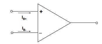
The difference between IB+ and IB- going into the terminals of an Op Amp can be defined as the input offset current. This difference in current will affect the voltage at this node.
Overvoltage Protection
The analog input circuitry has protection diodes in place that will gate a large voltage from damaging the most critical components of the device, such as the PGIA or ADC.
- When the device is powered on, these diodes are biased at some positive and negative voltage, meaning that a voltage larger than the sum of the bias and reverse voltage must be present before these diodes are overloaded and can be damaged.
- When the device is off, the bias voltage is removed, so the voltage needed to reverse the diodes is lower, making the device more susceptible to being damaged.
Example
The NI PXIe-7847R has protection up to ±42 V for AI pins. While the device is off, there is a lower level of protection at ±35 V.
Maximum Working Voltage
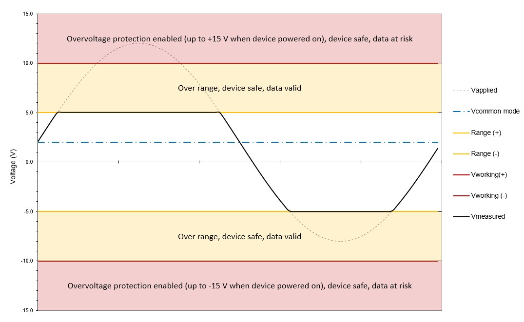
Maximum working voltage specifies the total voltage level that a device can tolerate on any analog input channel before data validity on other channels becomes an issue. The combination of the signal to be measured and any common mode voltage with respect to AI GND should not exceed this maximum working voltage specification to guarantee accuracy on other channels. Note that the maximum working voltage is independent of the input range of the device.
Example
A 10 Vpk sine wave with 2.0 VDC common mode is being measured on a PXIe-7847R, which has a maximum working voltage of ± 10 V when the AI is configured to a ± 5 V range, as shown below:
The combination of the two signals peaks at +12.0 V, which exceeds the maximum working voltage.
See Also
Overvoltage Protection
Input Range
Common Mode Rejection Ratio (CMRR)
When the same signal is seen on the positive and negative inputs of an amplifier, the CMRR specifies how much of this signal is rejected from the final output (typically measured in dB). An ideal amplifier will remove 100% of the common mode signal, but this is not achievable in implementation.
Example
The NI PXIe-7847R has a CMRR of -100 dB from DC to 60Hz. This means that it will attenuate common mode voltages by 100,000x. If the signal being measured is a 5 Vpk sine wave, and the offset or common voltage between the positive and negative inputs is 5 VDC, the final output will reject or attenuate the 5 VDC input to 5 µV. CMRR is not included in accuracy derivations and should be accounted for separately if the signal measured contains common mode voltages.
Small Signal Bandwidth
The range of frequencies that is passed with attenuation less than –3 dB. Tests for small signal bandwidth are made with low voltage signals so that slew rate distortion is not a factor.
Example
The NI PXIe-7847R has a small signal bandwidth of 1 MHz.
Large Signal Bandwidth
The range of frequencies that is passed with attenuation less than –3 dB. Tests for large signal bandwidth are made with full power signals where slew rate distortion is a factor.
Example
The NI PXIe-7847R has a large signal bandwidth of 500kHz MHz.
Crosstalk
The measure of how much a signal on one channel can couple onto, or affect, an adjacent channel. Crosstalk exists any time an amplitude-varying signal is present on a wire or PCB trace that is physically close to another wire or PCB trace.
Example
The NI PXIe-7847R has a crosstalk specification of -80 dB tested from DC to 100kHz, at 50 Ω termination.
Analog Output
Update Time
For analog output, update rate specifies how often in time the module produces an output. It is tied closely to maximum update rate
Maximum Update Rate
For analog output, update rate specifies how many samples per second the DAC to analog voltage or current values. Most NI devices have a single DAC per analog output channel, but will all share the FIFO where the analog output data is stored. The rate at which data can be read from this FIFO and transferred to the different DACs on board can sometimes limit the update rate when using multiple AO channels on the same device. Update rate is measured in samples per second (S/s).
For the analog input equivalent, see Sample Rate.
Example
The NI PXIe-7847R has eight analog output channels.
- The maximum update rate is 1MS/s
Type of DAC
Digital to analog converters can have different architectures. This specification will tell you what type of DAC was used in the product design.
Example An enhanced R-2R digital to analog converter uses the common concept of using a resistor ladder network to convert a digital signal into an analog voltage
Output Impedance
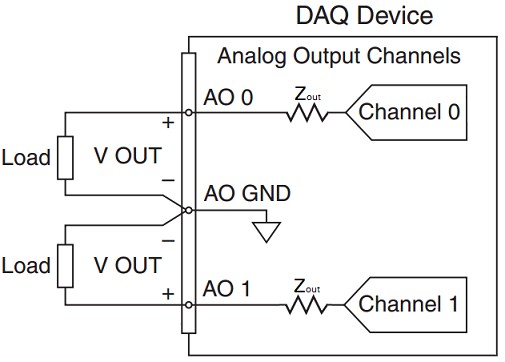
Output Impedance is the impedance that is effectively in series with an analog output channel, as illustrated below:
A low output impedance allows more of the voltage generated to be dropped across the load of the analog output. It is important to take the output impedance into account to ensure that the voltage level desired is achieved.
Example
The NI PXIe-7847R has an output impedance of 0.5 Ω. This means that if a load connected has an impedance of 500 Ω, and the voltage specified by the user is 1 V, the actual voltage on the load would be 0.999 V, or 1.0 mV, less than expected. At this voltage, there will also be 1.99 mA drawn from the device.
Output Current Drive
For analog output, output current drive is the maximum amount of current that the device can sink or source. The load that is connected, including output impedance, combined with the voltage programmed determines the current that will be required to maintain programmed output voltage.
Programmed output voltage is guaranteed if current drive remains below the specified output current drive. Exceeding output current drive puts the device into an overdrive state, where output voltage is no longer guaranteed.
Example
The NI PXIe-7847R is capable of driving ± 2.55 mA from any analog output channel. On the ± 10 V range, this means that the lowest total impedance that can be driven at full scale is determined from the highest power output, or largest current & voltage:
Taking into account the output impedance of the PXIe-7847R, the lowest connected impedance that can be driven at full scale is the difference of the minimum load and the output impedance:
Protection
Protection on the analog output pins will be defined by the protection circuitry implemented in each design. This could protect against current fly back spikes, or accidental shorts. But please refer to the individual specification sheet.
Example
Short circuit to ground protection has been implemented in the PXIe-7847R internal protection of the card against an accidental connection between an AO channel and GND. In which case we would expect a current spike, the module has protection against damaging itself in this case.
See also Overvoltage Protection and Overcurrent Protection
Overvoltage Protection
The analog output circuitry has protection circuitry in place that will provide protection against input voltages up to a certain voltage, specified by the module.
Example
The NI PXIe-7847R has protection up to ±15 V for A0 pins. While the device is off, there is a lower level of protection at ±10 V. The 5V lines have ±30 V protection
Power-on State
Power-on state specifies the value of an analog output channel when the device has powered on and after a glitching period known as the power-on glitch. Prior to the device receiving power from the bus, the value on the output is described in the power-on glitch specification.
Example
The NI PXIe-7847R will have the analog output channels as user configurable upon power-on.
Power-on Glitch
When applying and removing power from the device, there is a glitch signal on the analog output channels.
- Glitch Energy Magnitude—The peak amplitude that a glitch signal reaches during a glitch period
- Glitch Energy Duration—The length of time for the glitch signal to subside within the power-on state
Example
The NI PXIe-7847R has a specified glitch of 1 V for 1 µs.
Monotonicity
Monotonicity is the guarantee that when DAC codes increase, the output voltage also increases.
Example
The NI PXIe-7847R guarantees that the output voltage increases as DAC codes increase. For example, a ramp function will always either increase or decrease depending on the direction of the ramp.
Settling Time
The amount of time it takes for an analog output value to stabilize to within a certain degree of precision.
Example
The NI PXIe-7847R has a settling time of a full-scale step to within ±16 LSB of 5.3 µs. This means that for a full-scale oscillation on the ±20 V step size (V) the maximum frequency that can be driven to within 16 LSB is 1/(5.3 µs) = 188.68 kHz.
Slew Rate
Slew rate specifies the rate of change for the analog output channels in a given device. It is typically measured in V/µs. Settling time for output is calculated with slew time already included in the calculation. It is important to consider slew rate when designing a system for high amplitude high frequency signals, as the large swing in amplitude may exceed the slew rate for a given device.
Example
The NI PXIe-7847R has a typical slew rate of 10 V/µs, this means that the highest frequency at the ±5V scale that can be generated is 1 MHz. This number was calculated by taking calculating the frequency from time (freq=(1/t)). Knowing that the range of ±5V is 10V, and knowing that the slew rate is 10 V/µs, we can calculate that the highest frequency is (1/ 1µs) or 1MHz. Attempting to output a full scale signal with higher amplitude will result in unwanted distortion.
Glitch Energy at Midscale Transition
Glitch energy at midscale is produced by the DAC. The reason these glitches occur is that inherently in the DAC, when the Most Significant Bit (MSB) is switched in the middle of the range of the DAC the internal circuitry will produce a glitch. It is specified similarly to a power on glitch, and is an integral of the voltage over time.
Example
The PXIe-7847R has a glitch energy at midscale of ±10mV for 3 µs.
5V Output
Output Voltage
The 5V line will have a tolerance related to what voltage range is considered acceptable coming from the 5V pin.
Example
The PXIe-7847R is considered within specification if the 5V pin outputs voltage in the range of 4.75V to 5.1V.
Output Current
The output current specification in regards to the 5V output, is to let the user know that there is a limit on the amount of current that pin can source.
Example
If a user is wanting to use the 5V pin as an excitation line to power one of their sensors, that should be fine assuming that the load of the sensor is large enough to guarantee the module does not reach its specified current limit for the 5V pin. For example the PXIe-7847R has output current of 0.5A maximum from the 5V pin.
If V=IR, and V=5, and I must satisfy I < 0.5, then R, the resistance of the load must be at least 10 Ω.
Overvoltage Protection
Covered in overvoltage protection section under analog output
Overcurrent Protection
The current limit condition that will cause the module to go into an overcurrent state.
Example
The PXIe-7847R has an overcurrent protection at 650mA. So at this value the board will go into a overcurrent state.
Digital Subsystem Specifications
Digital I/O
Maximum Frequency
This is the maximum rate that the module can sample/generate DIO signals reliably.
Example
The PXIe-7847R has a maximum frequency of 10MHz on Connector 0, and 80MHz on Connector 1. For other modules such as the PXIe-7822R it has a maximum frequency of 80MHz on all 4 connectors. The 80MHZ frequency is being achieved on dedicated DIO connectors, which were validated using cabling and breakout boxes specifically designed for DIO signals (RDIO2 cable and HSDIO terminal block) to address crosstalk and noise concerns for digital signals. However for the PXIe-7847R connector 0, uses a RMIO cable and SCB-68A terminal block which also carries analog signals, and was not designed specifically for digital signals. Therefore, while the DIO channels in connector 0 can be pushed past 10MHZ in SW, the signal integrity may degrade due to crosstalk and other factors.
Compatibility
Digital I/O compatibility is the set of logic standards that the NI R Series module/card can adhere to. There are many different standards for logic levels. Some of the more common are TTL, CMOS, ECL, LVTTL, LVCMOS.
Example
The PXIe-7847R can function at LVTTL and LVCMOS
Input High Voltage / Input Low Voltage (VIH / VIL)
The recommended operating voltage ranges that an input signal should be in order to register a logic high or logic low. The logic family sets the thresholds for Vil (voltage input low maximum) and Vih (voltage input high minimum) which define the logic levels and that correlate to a logical high (1) or low (0). In between these two levels is undefined.
Example
The PXIe-7847R has logic families of 1.2, 1.5, 1.8, 2.5, and 3.3V, and each family has a corresponding Vil and Vih, that can be found in the specifications.
Minimum Input
The lowest voltage value that should be input into the NI R Series module/card digital pin.
Maximum Input
The highest voltage value that should be input into the NI R Series module/card digital pin.
Input Leakage Current
Ideally an input pin has infinite impedance and no current flow, however in reality the input will have a large impedance (but finite) that will result in a very small current flow. The input leakage current is a result of all the components impedance and the current that results. The way in which this is specified by NI is that there is a maximum current that could be a result of leakage.
Example
The PXIe-7847R has a maximum input leakage current of ±15 µA.
Input Impedance
Input impedance is a measure of how the input circuitry impedes current from flowing through to the digital input COM.
Example
The input impedance of the PXIe-7847R is 50kΩ typical. A case where input impedance becomes something that you must consider is if the source has a large output impedance. Take the hypothetical case where a sensor has an extremely high output impedance, such as 30 kΩ. Connecting the NI module to a sensor with this extremely high output impedance causes a 3 V nominal output from the sensor to be read as 1.875 V which could potentially be undefined at that voltage level.
Output High Voltage (VOH), or Output Low Voltage (VOL), or Output Voltage
The operating voltage ranges that can be expected from an output signal when generating a logic high or logic low. The output voltage generally also specifies the amount of current that the module can sink/source and maintain the high or low output voltage.
Maximum DC Output Current Per Channel
The maximum guaranteed current that the module can drive from all the input/output lines without going into an overcurrent state. This can depend on the voltage family
Example
The PXIe-7847R can source/sink a maximum of 4mA at the 3.3 V logic family.
Output Impedance
Output impedance is the impedance that is effectively in series with a digital output channel. A low output impedance allows more of the voltage generated to be dropped across the load. It is important to take the output impedance into consideration to ensure that the voltage level desired is achieved. The output impedance with output current can be used to determine the expected output voltage.
Example
The PXIe-7847R specifies an output impedance of 50 Ω. Therefore if a load was connected with a impedance of 500 Ω then the voltage that load would be subject to, assuming a 3.3 V output would be 3 V.
Power-on State
State of a DIO line when the module powers on. The state could be a digital input output, and furthermore a high, low, high impedance, etc… based off the states available to the module during start up.
Example
You can configure the NI 78xxR DIO lines individually for either input or output. When the system powers on, the DIO lines are at 50kΩ typical, pull down. To set another power-on state, you can configure the NI 78xxR to load a VI when the system powers on. The VI can then set the DIO lines to any power-on state
Protection
Individual digital lines have dedicated I/O protection against electrostatic discharge (ESD) and overvoltage conditions. NI recommends minimizing long-term over/under-voltage exposure to the Digital I/O. Prolonged DC voltage stresses that violate the maximum and minimum digital input voltage ratings may reduce device longevity. Over/under-voltage stresses are considered prolonged if the cumulative time in the abnormal condition exceeds 1 year
Digital I/O Voltage Selection
Each connector must have a logic family associated with its DIO. This is programmable in SW, but is defined at compilation (not at run-time).
Direction control of digital I/O channels
This determines whether each line, port, or connector can be defied as either a digital input or output.
Example
The NI-7847R can be defined as a digital input or output by channel.
Minimum I/O Pulse Width
Minimum I/O pulse width is the minimum amount of time that an I/O state must be enacted for the state to complete and be stable. Said in another way, a digital state must be constant for the length of time defined by the minimum I/O pulse width.
Example
The PXIe-7847R has a minimum I/O pulse width of 6.25ns, therefore a full cycle would take 12.5ns. If you find the inverse, it is 80MHz.
Minimum Sampling Period
This can be defined as the maximum timebase supported by the FPGA to sample the DIO signal.
Example
The PXIe-7847R has a minimum sampling period of 5 ns. If we know the frequency is equal to the inverse of time. Then we can calculate the maximum timebase that is supported by the FPGA of the PXIe-7847R to be 200MHz.
External Clock
Maximum Input Leakage
Characteristic Impedance
This is the amount of equivalent resistance of a transmission line if it were infinitely long, attributable to the distributed capacitance and inductance as the voltage and current “waves” propagate along the cable’s length.
Example
The PXIe-7847R has a characteristic impedance of 50 Ω on the external clock. This implies that if you are going to be routing an external clock into the device that the cabling and termination be impedance matched at 50 Ω for best results, that will minimize reflections.
Power-on State
See Power-on State
Minimum Input
See Minimum Input
Maximum Input
See Maximum Input
Logic Level
A logic level is generally defined by a standard but will be the voltage level at which an input will be registered as a high (1) or a low (0). This topic is closely related to the compatibility section.
Maximum Input Frequency
The maximum frequency that can be routed into the external clock
Other Specifications/Terminology
Reconfigurable FPGA
Field Programmable Gate Arrays are reprogrammable silicon chips. To learn more about this please read through other NI resources. (NI FPGA)
Some other common terminology when using FPGA's, include:
Flip-flops: also sometimes referred to as registers
LUT: Look up table
Onboard DRAM
Dynamic random-access-memory. This is a type of RAM that stores each bit of memory inside of separate tiny capacitors within an integrated circuit. These capacitors can hold a charge (1), or be discharged (0), however since these are capacitors they will leak electric charge if not refreshed. Therefore all of this memory is volatile, and is lost quickly after a loss of power.
Synchronization Resources
Depending on the device and form factor (PCI/PCIe, PXI/PXIe) there will be various synchronization options open. Generally defined by NI as input or output sources. The sources are will be defined by the form factor and the routing available for each module. If you are looking to distribute synchronization pulses to or from the module these sources are useful.
Example
The PXIe-7847R has typical PXIe routing lines that are built into the backplane of a PXIe chassis. These will include PXI_Star lines with are trace length matched, PXI_Trig lines which are bidirectional, as well as access to the backplane clock sources.
Bus Interface
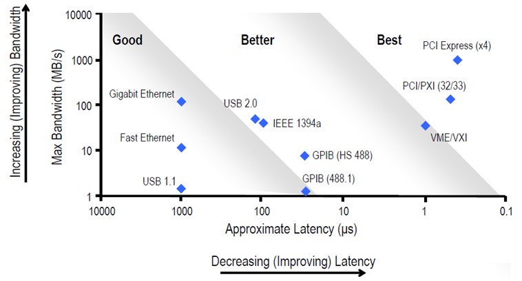
PCI, PCI Express, PXI, PXI Express, and USB are all examples of bus interfaces that an MIO DAQ device may take. These buses provide some key tradeoffs between data throughput, latency, portability, and channel count.
Example
The NI Multifunction Reconfigurable I/O (R Series) comes in USB, PXI Express, and PCI Express. While these devices and modules have similar functionality, the PXI Express module and PCI Express device provide lower latency and higher throughput compared to the USB device. The PXI Express module has the additional benefit of the PXI Express system. The USB device has the benefit of being hot-swappable and more compact, making it better for mobile applications.
Maximum Power Requirements
It is important to know the power requirements of USB and PCI devices or PXI modules so that the correct amount of power can be sourced. The values indicated in this section are for normal use and do not show the maximum power that a device or module can draw if used outside of specifications. For USB devices, an NI-supplied power supply meets the recommended specifications, but you can use a third party or custom supply if needed. For PCI or PCI Express devices, there is a disk drive power connector that may be used in case more power is needed. This is most common when using the +5 V user rail for powering an external circuit. Refer to current limits for more information. For PXI or PXI Express modules, this specification is useful when making a power budget. Refer to the related links for more information.
Example
The PXIe-7847R draws 3 A from the +3.3 V rail and 2 A from the +12 V rail. So the total power consumed will be calculated using P = I*V. Therefore the total power consumption from the PXIe module is 33.9 W.
See Also
Performing a Power Budget on a PXI System
Physical Characteristics
NI publishes dimensional drawings of most products that can be used to check clearance prior to purchasing a device or creating a model of the system being created. In addition to dimensions, NI also provides a comprehensive list of custom cabling, connectors, and screws.
See Also
Dimensional Drawings
NI DAQ Device Custom Cables, Replacement Connectors, and Screws
Maximum Working Voltage
Please see the other Maximum Working Voltage section. However please pay attention to the Measurement Category rating and the caution/notes included within this section of the manual as they will provide guidance on safety and proper use.
Safety, Electromagnetic Compatibility, CE Compliance
The standards that Reconfigurable MIO (R Series) devices are tested and in compliance with are listed out in the three sections in our specifications manuals. For more information on any standard, visit Product Certifications.
Example
You can view the compliance specifications for the PXIe-7847R by using the certifications search: PXIe-7847R
Shock and Vibration
Reconfigurable MIO (R Series) devices are tested to specific industry standards to ensure that stated accuracy according to the specifications and device integrity is maintained over the stated shock and vibration specifications. It is important not to exceed these specified values to ensure correct and accurate operation of the device.
Example
The PXIe-7847R was tested in accordance with IEC 60068-2-64 and the test profile developed in accordance with MIL-PRF-28800F Class 3.
Calibration
Like all test and measurement equipment, it is important that routine calibration is performed to ensure that the device is operating within the specified accuracy settings. The device has some amount of self-heating, so it is important to allow the specified warm-up time prior to taking any measurements to ensure a stable temperature is reached. At this point, it is recommended that the device is self-calibrated if supported. Refer to Calibration Services for more information about the calibration services that NI offers.
Example
The PXIe-7847R has a 15 minute warm-up time and a calibration interval of 1 year. NI recommends self-calibrating the device after 15 minutes of being powered on to ensure optimal accuracy. After one year of use, NI recommends sending the device in for a certified calibration. For solely digital modules (PXIe-782XR) there is no calibration interval or procedure. The recommendations around general care and self-calibration hold true for all NI module.
Additional Resources
- Multifunction Reconfigurable I/O Device product page
- PXI Multifunction Reconfigurable I/O Device product page
- Getting Started with R Series Multifunction RIO
- Getting Started With NI R Series for USB Part 1: Introduction
- NI R Series for USB Getting Started Part 2: Advanced
- NI R Series Multifunction RIO Frequently Asked Questions (FAQ)
- NI 78xx Models: R Series Cable and Accessory Compatibility
- Software Support for CompactRIO, CompactDAQ, Single-Board RIO, R Series, and EtherCAT
