Specifications Explained: NI Oscilloscopes and Digitizers
Overview
Contents
- Introduction
- Understanding Specification Terminology
- Vertical
- Horizontal
- Triggers
- TClk Specifications
- Waveform Specifications
- Additional Resources
Introduction
This guide is broken up into the same sections as most NI specifications manuals. Terms and definitions below are listed in alphabetical order and may occur in a different order in the specification manuals. This guide exclusively applies to 51xx families, USB, PCI, PXI and PXIe Oscilloscope and Digitizer devices and modules. Other NI product families such as Multifunction DAQ 60xx, 61xx, 62xx, and 63xx families (formerly B, E, S, M, and X Series), cDAQ and cRIO Chassis and Controllers, C Series Modules, Multifunction RIO 78xx R Series, Digital Multimeters, and other instruments may use different terminology or methods to derive specifications and as such, this guide should not be used as a reference for devices and modules other than those in the NI Oscilloscope and Digitizer families.
This guide will use the PXIe-5162 for many of the references throughout. If you would like to follow along with those device specifications, you can do so by following this link: PXIe-5162 Specifications. If the specification references another Oscilloscope or Digitizer, you can follow along by navigating to the device's specifications as well.
Understanding Specification Terminology
First, it is important to note the categorical difference between various specifications. NI defines the capabilities and performance of its Test & Measurement instruments as either Warranted Specifications, Typical Specifications, or Nominal Specifications. See your device's specifications manual for more details on which specifications are warranted, typical or nominal.
- Warranted specifications describe the performance of a model under stated operating conditions and are covered by the model warranty.
- Typical Specifications describe the performance met by a majority of models. Typical specifications are not warranted.
- Nominal Specifications describe an attribute that is based on design, conformance testing, or supplemental testing. Nominal specifications are not warranted.
Vertical
NI Oscilloscope and Digitizer devices and modules have specifications for analog signals. These specifications can be unique for each device or model, so be sure to check the specifications for your specific model. This section is organized in six sections to cover the common specifications: Impedance and Coupling, Voltage Levels, Accuracy, Bandwidth and Transient Response, Spectral Characteristics, and Noise.
Impedance and Coupling
Input Capacitance
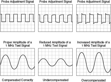
Digitizer inputs have parasitic capacitance that can potentially alter the signal being measured. A probe with an adjustable capacitance can be used to compensate for the input capacitance and achieve a flat frequency response. When frequencies are low, the capacitance has a very high reactance which does not cause meaningful loading. However, as the frequency increases, the loading becomes much greater due to a decrease in the probe's impedance.
Figure 1 shows a correctly compensated, undercompensated, and overcompensated probe for low frequencies. It should be noted that the cable capacitance is also compensated when the probe is compensated.
Figure 1
Example
The PXIe-5172 has a typical input capacitance of 16 pF ± 1.2 pF for 1 MΩ input impedance. The probe used needs to be able to compensate from 14.8 pF to 17.2 pF for best results
Input Coupling
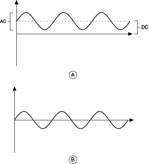
You can specify an input channel to be DC-coupled, AC-coupled, or ground coupled. DC-coupling allows DC and low frequency components of a signal to pass through without being attenuated. AC-coupling removes DC offsets and low frequency components, only allowing high frequency signals. Ground coupling disconnects the input and internally connects the channel to ground to provide a ground, zero-voltage reference.
In Figure 2, Plot A shows DC-coupling that shows the waveform with the DC portion included. Plot B shows the same waveform with AC-coupling that removes the DC component.
Figure 2
Example
The PXIe-5164 has both AC and DC coupling to allow both low and high frequency signal measurements.
Input Impedance
Input impedance is a measure of how the input circuitry impedes current from flowing through to analog input ground. For NI Oscilloscopes, the common input impedance is 50 Ω or 1 MΩ.
Typically, the 1 MΩ, or high Z, impedance is used with a probe for high voltage measurements. For some applications, such as RF, 50 Ω input impedance is used to match the source impedance to minimize reflections that can distort the signal being measured.
Example
The PXIe-5164 has both 50 Ω and 1 MΩ input impedances. Choosing the appropriate input impedance is important for taking good measurements.
See Also
Select the Right Oscilloscope Probe for Your Application: Loading Effects
Input Return Loss
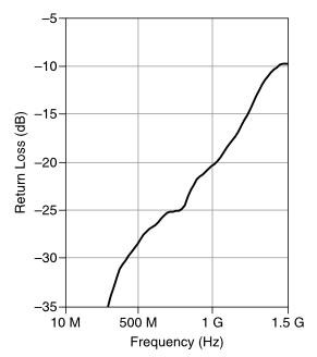
Input return loss indicates the decrease in power of a signal that is reflected due to mismatched impedances. The equation for return loss can be found below.
Example
The PXIe-5162 has an input return loss of roughly -20 dB for a frequency of 1 GHz. This means that a signal 20 dB less than the input signal is reflected due to impedance mismatch.
Figure 3
Input Voltage Standing-Wave Ratio (VSWR)
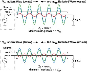
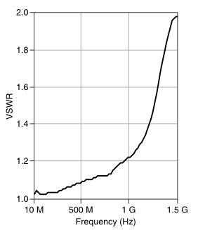
VSWR is the ratio of reflected vs. transmitted waves. VSWR can be used to determine how much of the input signal is being reflected. Depending on whether the reflected wave is in or out of phase with the input signal, it could either increase or decrease the net amplitude. VSWR is the ratio of this maximum net amplitude and minimum net amplitude. Different ways to find VSWR are shown in the equations and figures below.
ZL-Load Impedance
Zo-Characteristics Impedance
Figure 4
Example
The PXIe-5162 has a VSWR of roughly 1.1 at 500 MHz. This gives the ratio of the maximum amplitude and minimum amplitude due to the phase of the reflected signal.
Figure 5
See Also
Chapter 1: Understanding Key RF Switch Specifications: Voltage Standing-Wave Ratio
Voltage Levels
Input Offsets
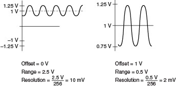
Input offset, or vertical offset, is the voltage on which the voltage range is centered. Vertical offset positions the vertical range around a user-defined DC value. Using this offset allows for examination of small changes in the input signal, which can lead to improved measurement accuracy.
Figure 6 shows the relationship between the input range and offset and how it can affect the resolution.
Figure 6
Example
The PXIe-5164 has an input offset of ±5 V for the 0.25 V input range. This allows the oscilloscope to measure a signal that is carried by a ±5 DC voltage to fully maximize the ADC's performance.
Input Ranges
Input range, or vertical range, is the peak-to-peak voltage span that a digitizer can measure at the input connector. Many digitizers have multiple vertical ranges to maximize the ADC's performance and get better resolution.
Example
The PXIe-5171 has input ranges of 0.2 Vpp, 0.4 Vpp, 1 Vpp, 2 Vpp and 5 Vpp. A user has these five ranges to choose from to get the best possible resolution. If the signal being measured is 0.5 Vpp, it would be best to use the 1 Vpp range rather than the 5 Vpp range to maximize the ADC.
Maximum Input Overload
This is the maximum input voltage that a device can handle. Exceeding this voltage may cause damage to the device.
Example
The PXIe-5162 has a maximum input overload of |Peaks| ≤ 42 V for 1 MΩ. The maximum input range for the device is 50 Vpp with a ±15 V offset. This means input signals with peaks of ±40 V can be measured and still be within the input overload specification of 42 V.
Accuracy
AC Amplitude Accuracy/Frequence Response
Since real-world amplifiers cannot provide ideal performance, the gain is a product of the input frequency. Frequency response gives the magnitude response of a signal over a range of frequencies.
Figure 7
Example
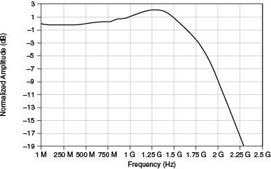
Consider a signal of 1.25 GHz acquired on the PXIe-5162 with a 50 Ω input impedance and 1 Vpp range, the equation above for AC amplitude accuracy and Figure 7, the frequency response graph, can be used to find the typical accuracy. Figure 7 shows an amplitude of roughly 2 dB for 1.25 GHz signal, taking the accuracy as 2 dB ± 0.5 dB, or the range 1.5 dB to 2.5 dB.
AC Amplitude Drift
Like DC drift, the AC amplitude can drift due to a change in temperature from the last calibration.
Example
The amplitude drift of the PXIe-5162 can be found using the equation from its specification document. Taking the example from the AC Amplitude Accuracy section, if the board temperature is now 5 degrees from the calibrated temperature, the AC amplitude now falls within the range 1.48 dB to 2.52 dB. The AC amplitude accuracy changes by just 0.02 dB because the PXIe-5162 only takes temperature changes beyond ± 3·°C into account for AC amplitude drift.
Crosstalk
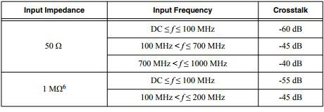
Crosstalk is the measure of how much a signal on one channel can affect another channel. Ideally, acquiring a signal on one channel should not affect another signal being acquired, but this is not always the case due to unwanted conductive, capacitive, or inductive coupling from one part of the digitizer to another.
Example
The Channel-to-Channel Crosstalk table from the PXIe-5162 specification document shows that if a signal of 50 MHz is being sampled with an input impedance of 50 Ω, there is a characteristic isolation of -60 dB between channels when both are set to the same input range.
Table 1
DC Accuracy
Accuracy determines how close the value given by the digitizer will be to the actual signal.
Example
The equation below shows the DC accuracy specification from the PXIe-5162 specification document. An example of calculating the DC accuracy of a signal that is 0.6 V with 0 V vertical offset and a full-scale voltage of 1 V is shown below.
DC Drift
DC drift is used to find the accuracy of the digitizer when the onboard temperature of the device is more than ±X °C since it was last calibrated.
Example
X varies from device to device; on the PXIe-5162 it is 3 °C. The equation above shows the DC drift spec from the PXIe-5162 Specification document. An example of calculating the DC drift of a 0.6 V signal with a 0 V vertical offset, full-scale voltage of 1 V, and a difference in onboard temperature of 5 ℃ from the last calibration is shown below.
Resolution
Resolution is the smallest input voltage change a digitizer can ideally capture. Resolution can be expressed in bits (LSB), in proportions, or in percent full scale. Table 2 gives a few examples.
| Bits | Resolution | ||
|---|---|---|---|
| 8 | 1/28 | or | 1/256 |
| 10 | 1/210 | or | 1/1024 |
| 12 | 1/212 | or | 1/4096 |
| 14 | 1/214 | or | 1/16384 |
| 16 | 1/216 | or | 1/65536 |
Table 2
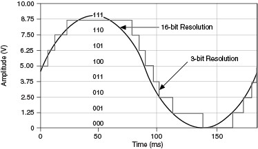
Resolution limits the precision of a measurement. The higher the resolution (number of bits), the more precise the measurement. An 8-bit ADC divides the vertical range of the input amplifier into 256 discrete levels. With a vertical range of 10 V, the 8-bit ADC cannot ideally resolve voltage differences smaller than 39 mV. In comparison, a 14-bit ADC with 16,384 discrete levels can ideally resolve voltage differences as small as 610 µV.
Figure 8 shows a sine wave measured by a 3-bit ADC and a 16-bit ADC.
Figure 8
Example
The PXIe-5160 has a 10-bit resolution, which gives it 1,024 discrete levels. Given a 10 V range, this allows the device to measure changes as small as 9.77 mV. In comparison the 3-bit resolution in Figure 8 can only measure changes of 1.25 V.
Bandwidth and Transient Response
AC-Coupling Cutoff
The AC-coupling cutoff gives the -3 dB point of the high-pass filter when using AC coupling.
Example
The PXIe-5162 has a cutoff of 170 kHz for 50 Ω and 17 Hz for 1 MΩ. When using 1 MΩ input impedance with AC coupling, frequencies below 17 Hz will be attenuated by more than 3 dB.
Bandwidth
Bandwidth is defined as the point when the measured signal’s power is half of the original signal’s power. When working with a voltage signal, the -3 dB point is when the measured voltage is times the original. Since NI Digitizers pass DC, the bandwidth is specified as the uppermost frequency that can be measured before the signal hits
times the original value.
Example
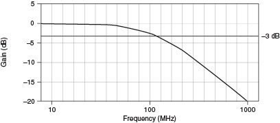
The PXIe-5162 has a bandwidth of 1.5 GHz in the 50 Ω input impedance setting and 300 MHz in the 1 MΩ setting. The warranted 50 Ω case indicates that the input signal will not be attenuated to 70.7% when the frequency of the input signal is under 1.5GHz. Figure 9 shows that the -3 dB point is roughly 150 MHz for a particular digitizer.
Figure 9
See Also
Acquiring an Analog Signal: Bandwidth, Nyquist Sampling Theorem, and Aliasing
Bandwidth-Limiting Filters
Bandwidth filters are used to filter out undesirable spurs and noise to achieve improved resolution on the input signal. These filters can be thought of as low-pass filters that are used to reject unwanted high frequency content associated with the input signal. These filters can be analog or digital.
Example
The PXIe-5162 has two bandwidth limiting filters, 20 MHz and 175 MHz. When measuring a 15 MHz signal, the 20 MHz filter would be used to keep out unwanted high frequencies. For a signal of 150 MHz, the 175 MHz filter can be used.
Frequency Response
Frequency response gives the magnitude response of a signal over a range of frequencies. This shows how the magnitude of input frequencies will vary for each oscilloscope.
Example
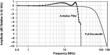
Figure 10 shows the frequency response of the PXIe-5105 in the 50 Ω, 1 Vpp input range at full bandwidth with the anti-alias filter enabled.
Figure 10
Rise/Fall Time
The rise/fall time indicates the slew rate, the fastest transition the digitizer can measure.
Example
For example, the PXIe-5172 can measure signals that rise as fast as 5.15 ns in the 50 Ω range and 5.25 ns in the 1 MΩ range nominally.
See Also
Acquiring an Analog Signal: Bandwidth, Nyquist Sampling Theorem, and Aliasing
Spectral Characteristics
Effective Number of Bits (ENOB)
ENOB is a specification that relates measurement or generation performance of a device to a common specification used in data converters: bits of resolution. Most data converters are designed to perform at a particular speed and resolution. Instrument vendors have always used this design element to define the measurement resolution of their devices. No instrument is ideal, so performance specifications show how close a device is to ideal. An ADC may specify a certain number of bits, but noise may add measurement uncertainty that exceeds the precision those bits could ideally achieve. For example, a 14-bit ADC may only have 12 usable bits: this is the ENOB of the device. ENOB is calculated directly from SINAD, discussed below, using values for ideal ADC noise and spurs as shown in the equation below. This calculation shows how close to an ideal instrument the device is performing. ADC performance declines as the input frequency increases due to high-frequency distortions; this causes ENOB to diminish with increasing input frequency.
Example
The PXIe-5172 has an ENOB of 11.8 bits when the 20 MHz filter is enabled in the 5 V range. Even though it is a 14-bit product, under those conditions it has an ENOB of 11.8
Signal-to-Noise-and-Distortion (SINAD)
SINAD is the ratio of signal power, including noise and distortion power, to noise and distortion power alone. An instrument with high SINAD can discern the fundamental frequency from spurs and noise better than an instrument with a low SINAD. The most useful approximation of SINAD is shown in the equation below.
Example
Using ENOB, we can calculate SINAD. Using the example and equation in the ENOB section above gives the PXIe-5172 a SINAD of 72.796 dB.
See Also
Signal-to-Noise Ratio (SNR)
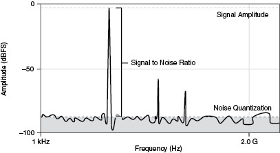
SNR, usually given in dB, is the ratio of the power of the input signal level to the noise power. The greater the SNR of a device, the better its ability to differentiate between the signal and noise, especially when the input signal has a low amplitude.
Figure 11
Example
Based on the single-tone spectrum of the PXIe-5162 as shown in Figure 11, SNR can be approximated as 91 dB.
Single-Tone Spectrum
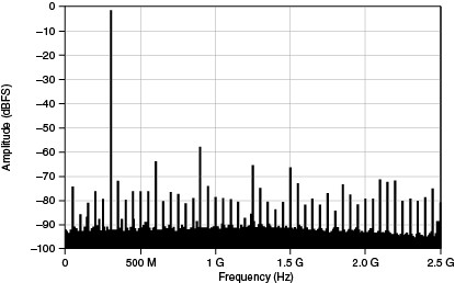
The single-tone spectrum uses a pure tone input signal to represent an oscilloscope's overall spectral performance.. A single-tone spectrum provides a good approximation of spectral characteristics such as THD, SNR, and so on for a specific configuration.
Example
Figure 12 displays the single-tone spectrum of the PXIe-5162 when tested with an input signal of approximately 300 MHz.
Figure 12
Spurious-Free Dynamic Range (SFDR)
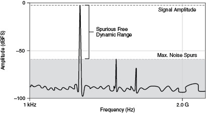
Spurious free dynamic range (SFDR), usually expressed in dBc, is the usable dynamic range before spurious noise interferes with or distorts the fundamental signal. The amplitude of the fundamental signal is usually -1 dBFS. SFDR is the measure of the ratio in amplitude between the fundamental signal and the largest harmonically or non-harmonically related spur from DC to the full Nyquist bandwidth (half the sampling rate). A spur is any frequency bin on a spectrum analyzer, or from a Fourier transform, of the analog signal above the noise floor. A device with a high SFDR can measure a signal with less effects from noise and spurs.
Figure 13
Example
The PXIe-5171 has a characteristic SFDR of -70 dBc or better, depending on filters, voltage range, and input frequency. This means that the highest noise spur is at least 70 dBc below the fundamental frequency.
Total Harmonic Distortion (THD)
The THD of a signal is the ratio of the sum of the powers of the first five harmonics to the power of the fundamental frequency. The equation below shows the calculation for THD, where H is the amplitude of each harmonic and F is the amplitude of the fundamental frequency.
Example
The PXIe-5172 has a THD of -77 dBc for an input frequency of 30 MHz or less in the 5 V input range.
See Also
Noise
RMS Noise
All voltage and frequency components that are not present in the actual or ideal signal, spurs, or harmonics, but are present in the measurement of signals, are noise. Input signals not only carry the ideal signal that needs to be measured, but also contain noise. The noise floor is the amplitude of any noise in the device’s frequency range. RMS noise indicates the noise that can be seen depending on factors such as input impedance and input range. The RMS noise of an oscilloscope is the noise present without an input signal and measured with a 50 Ω terminator.
Example
The RMS noise of the PXIe-5164 configured for 50 Ω of input impedance and 5 V input range is 0.030.
Horizontal
The following section is organized into two sections, Sample Clock and Onboard Clock (Internal VCSO). Each section contains a list of common specifications and their definitions and details how that specification might be used in the real world.
Sample Clock
Timebase Frequency
Timebase frequency is the basis of the clock used sample signals.
Example
The timebase frequency of the PXIe-5162 is 2.5 GHz. Sample clocks on the PXIe-5162 are derived from this 2.5 GHz frequency.
Onboard Clock (Internal VCSO)
Phase Noise
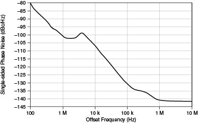
Ideal oscillators have a constant period and rise and fall times, but for actual oscillators, these features vary. These variations in the clock, called jitter in the time domain, can cause fluctuations in phase when measuring the input signal, resulting in phase noise in the frequency domain. Phase noise is given in dBc/Hz, where dBc is the level in dB with respect to the signal of interest.
Example
Figure 14 shows the phase noise plot for the PXIe-5162. Phase noise is -80 dBc/Hz when the frequency is 100 Hz and roughly -142 dBc/Hz when the frequency is 10 MHz.
Figure 14
Random Interleaved Sampling (RIS) Rate
RIS is a form of equivalent-time sampling that increases apparent sample rates of repetitive signals by combining several triggered waveforms, and the RIS rate is the sampling rate the digitizer can reach when using this method. Because the trigger time occurs randomly between two samples, the digitizer samples different points in the waveform on consecutive acquisitions. By combining these waveforms, The digitizer can reach a sample rate up to 25 times higher than the sample rate of its ADC. Not all NI oscilloscopes support RIS.
Example
The random interleaved sampling range for the PXIe-5162 is up to 100 GS/s.
See Also
High Speed Digitizers Help: Equivalent-Time Sample and Random Interleaved Sampling
Real-Time Sample Rate
Real-time sample rate is the actual rate at which the input signal is sampled.
Example
For the PXIe-5162 the real-time sample rate is the following:
One Channel Enabled: 76.299 kS/s to 5 GS/s
Two Channels Enabled: 76.299 kS/s to 2.5 GS/s
Four Channels Enabled: 76.299 kS/s to 1.25 GS/s
Sample Clock Jitter
Sample clock jitter indicates the deviation from the ideal sample clock. These deviations are described in Phase Noise above.
Example
PXIe-5162 has a sample clock jitter of 180 fs RMS, meaning a deviation of 180 fs from the ideal clock. This jitter value is calculated by integrating phase noise between two frequencies.
Timebase Accuracy
Timebase accuracy describes how close the actual frequency generated is to the desired frequency. The accuracy is given in ppm (parts per million) or ppb (parts per billion).
Example
The equation below uses the timebase accuracy of the PXIe-5162, 10 ppm, to determine the accuracy of a 1 MHz frequency.
External Sample/Reference Clock
Input Voltage Range Configured as Sample Clock
This value indicates the acceptable range for an external sample clock in dBm, the power of the input with respect to 1 mW.
Example
The PXIe-5162 has an input voltage range of -10 dBm to 16 dBm; the equation below converts this range to Vpp. Using this equation, the Vpp value of 16 dBm is found to be ~4 Vpp; this gives us a range of 0.2 Vpp to 4 Vpp.
Triggers
NI oscilloscope and digitizer devices and modules can support various types of triggering. They also support Programmable Function Interface (PFI) lines, which provide a way to route digital signals across the PXI/PXIe chassis backplane. The following is a list of common specifications, their definitions, and how those specifications might be used in the real world.
Dead Time
When acquiring multiple records, dead time is the total time between records that the digitizer is not acquiring. During this time, the digitizer is setting up for the next record.
Example
The dead time for the PXIe-5172 is 10 times the sample clock period. If the sample clock period is 4 ns, the dead time would be 40 ns.
Digital
A digital trigger occurs on a rising or falling edge of a digital signal.
Example
This could be a trigger that comes from a PFI line or a PXI trigger line.
Edge
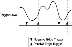
An edge trigger occurs when a signal crosses a user-specified threshold. The trigger can be either a positive (rising edge) or negative (falling edge) slope, as illustrated in Figure 15.
Figure 15
Hysteresis
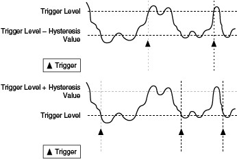
A hysteresis trigger is similar to an edge trigger, but adds a hysteresis value to prevent any false triggers. For a positive hysteresis trigger, the oscilloscope triggers when the set threshold has been crossed on a rising edge and won’t trigger again on the rising edge unless the signal drops below the hysteresis value. This prevents false triggers from a signal that may be jumping above and below the trigger threshold. Figure 16 illustrates a positive and a negative slope hysteresis.
Figure 16
Immediate
An immediate trigger is one that is generated by the digitizer itself after it is configured by software. This is the default for NI digitizers.
Software
A software trigger occurs when the user sends a software command to trigger the digitizer.
Time-to-Digital Conversion Resolution
This value lets the user know how accurately they can timestamp when the first sample was taken relative to when the trigger occurred.
Example
The time-to-digital conversion of the PXIe-5162 is 4 ps.
Trigger Accuracy
Trigger accuracy describes the range around the actual trigger value within which the oscilloscope trigger will activate..
Example
The PXIe-5162 has an accuracy of 8% of full scale. If the range is set to 5 V, the trigger accuracy is within 0.4 V. This means that for a 5 V setting the trigger will activate within the range of 4.6 V to 5.4 V.
Trigger Delay
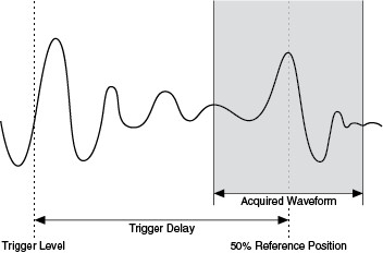
Trigger delay is the time that passes between when a trigger occurs and when the digitizer triggers. If a trigger delay is set, the digitizer continues to acquire pre-trigger samples for that set delay after it is triggered. Post-trigger samples are acquired after the delayed trigger.
Figure 17
Trigger Filters
Trigger filters are used to reject unwanted high frequency or low frequency components to prevent false triggers. For example, a low frequency trigger filter can be used to reject a 50 Hz or 60 Hz line signal. A high frequency trigger filter can be used to reject high frequency content such as overshoot and ringing.
Example
The PXIe-5162 has 150 kHz low frequency and high frequency reject filters so that unwanted frequencies below or above 150 kHz can be filtered out.
Trigger Holdoff
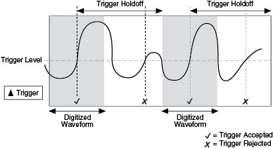
Trigger holdoff is an adjustable period during which the digitizer cannot trigger. Trigger holdoff is used to guarantee a minimum time between two reference triggers. This feature is useful if incoming triggers are a known time apart and only a relatively small window of samples adjacent to the trigger are necessary. In this case, setting the holdoff gives the ability to efficiently allocate the onboard memory and prevents the device from triggering on sections of the input waveform that are not of interest. Each device uses an onboard counter that is programmed by software to implement this functionality. While the holdoff counter is decrementing, incoming reference triggers are ignored. The device arms itself for the next reference trigger when the holdoff counter reaches zero. Each device that supports trigger holdoff has a minimum holdoff value, which is listed in the specifications document for each device.
Figure 18
Trigger Jitter
Trigger jitter is the possible deviation in ps of when a trigger occurred and when the digitizer reacted to it.
Example
The trigger jitter for the PXIe-5172 is 15 ps rms.
Trigger Sensitivity
Trigger sensitivity is the smallest voltage that causes the device to trigger.
Example
The PXIe-5162 has a sensitivity of 3% of full scale. If the range is set to 5 V, the trigger sensitivity would be 0.15 V.
Programmable Function Interface (PFI)
VIH
VIH is the minimum voltage level that can be interpreted as a “high” or “1” by a digital input.
Example
The VIH is 2 V for the PXIe-5162, which means that a minimum of 2 V must be input for the device to read a digital high.
VIL
VIL is the maximum voltage level that can be interpreted as a “low” or “0” by a digital input.
Example
The VIL is 0.8 V for the PXIe-5162, which means that a maximum input of 0.8 V can be input for the device to read a digital low.
Output Events
Ready for Start
A trigger when the digitizer is ready for a start trigger.
Start Trigger (Acquisition Arm)
A trigger when the digitizer receives a start trigger and begins acquiring minimum pre-reference trigger samples.
Ready for Reference
A trigger when the digitizer is ready for a reference trigger.
Arm Reference Trigger
A trigger when the digitizer has received an arm reference trigger.
Reference (Stop) Trigger
A trigger when the digitizer has received a reference trigger and is now going to acquire post-reference trigger samples.
End of Record
A trigger when the digitizer has completed acquiring a record.
Ready for Advance
A trigger when the digitizer is waiting to advance to the next record.
Advance Trigger
A trigger when the digitizer advances to the next record and begins acquiring minimum pre-reference trigger samples.
Done (End of Acquisition)
A trigger when the digitizer has finished acquiring samples and the acquisition is complete.
TClk Specifications
Skew
This is the maximum time delay between channels on separate modules.
Example
When using NI-TClk to synchronize multiple PXIe-5162 oscilloscopes, there will be a maximum characteristic delay of 100 ps between the channels of the modules.
Skew After Manual Adjustment
The sample clock can be manually delayed to improve the skew.
Example
The PXIe-5162 can reduce its skew down to ≤5 ps after manual adjustment.
Sample Clock Delay/Adjustment Resolution
This is the smallest increment the sample clock can be adjusted when manually adjusting skew between modules.
Example
The PXIe-5162 can delay the sample clock in increments of 20 fs to improve the skew when synchronizing using NI-TClk.
Waveform Specifications
Onboard Memory Size
The available memory the digitizer has to store acquired samples.
Example
The onboard memory size is 1.5 GB for the PXIe-5164.
Minimum Record Length
A record is a collection of samples, and minimum record length is the smallest number of samples that can be acquired per record.
Example
The minimum record length is 1 sample for the PXIe-5164.
Number of Pre-Trigger Samples
The number of samples that can be acquired before a reference trigger occurs.
Example
The number of pre-trigger samples is 0 up to (record length - 1) for the PXIe-5164.
Number of Post-Trigger Samples
The number of samples that can be acquired after a reference trigger occurs.
Example
The number of post-trigger samples is 0 up to the record length for the PXIe-5164.
Allocated Onboard Memory per Record
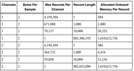
This number gives the amount of memory that a single record will use given a specific record length, and in some cases, the number of bytes per sample.
Example
Table 3 shows a few examples of this for the PXIe-5164 with 1.5 GB of onboard memory.
Table 3
