This section describes the necessary steps to reuse a project that was created based on the 802.11 Application Framework v1.1 (created in LabVIEW Communications 1.1) in LabVIEW Communications 2.0.
The section includes the following steps, each with their own subsection:
- Reconfigure the Xilinx IP cores
- Update “802.11 Internal Loopback Throttle Control.gcdl”
- Migrate to the new USRP interface
- Update host-side DMA FIFO’s
Reconfigure the Xilinx IP
Scope
Because the FPGA compile tools uses a new Xilinx Vivado Toolchain version, all Xilinx IP cores must be updated to the new version. By configuring the IP cores again, the dependencies are regenerated ensuring that they will be compatible with the latest Vivado version to ensure successful compilations.
Which Files are Affected?
- All FPGA GCDL files which include a Xilinx IP core
The affected files can be found by completing the following steps:
- Create a backup of your project.
- Open your project in LabVIEW Communications 2.0.
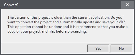
- Click Yes to convert as shown in Figure 1.

Figure 1: Convert? Dialog
- Open the FPGA top-level VI you wish to migrate, for example, “802.11 FPGA STA.gvi“
- Wait until type propagation has occurred.
- If the document finished loading, you will see in the list of errors the affected files as shown in

Figure 2: Error list showing affected files for Xilinx IP Core reconfiguration
Step-By-Step Instructions
- If not done already, make sure to back up the original project and convert a copy for use with LabVIEW Communications 2.0. For details, refer to steps 1-3 from the previous section “Which Files Are Affected?”
- Once open in LabVIEW Communications 2.0, open the FPGA top-level you wish to migrate, for example, “802.11 FPGA STA.gvi“
- Double-click on the errors, as shown in Figure 2. This will open the affected document.
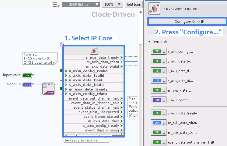
- Select the affected Xilinx IP block, and click on Configure Xilinx IP Core in the right-hand rail as shown in Figure 3.
- Wait for the “Re-customize IP“ dialog to appear.
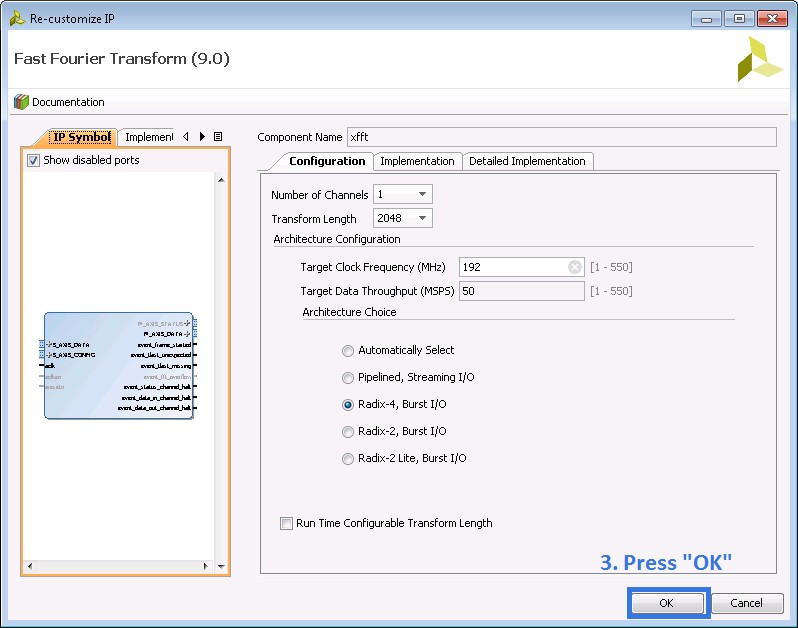
- Inside the “Re-customize IP“ dialog, leave the pre-configured settings untouched, and click OK as shown in Figure 4.
- Wait until the “Not Ready“ warning, as shown in Figure 5, has disappeared.
- Repeat steps 3 through 6 until all errors in the FPGA top-level are gone.

Figure 3: How to reconfigure a Xilinx IP Core

Figure 4: How to reconfigure a Xilinx IP Core (2)

Figure 5: "Not Ready" warning because Xilinx tool is processing the IP in the background
Update “802.11 Internal Loopback Throttle Control.gcdl”
Scope
Some changes in the Xilinx Vivado toolchain make it necessary to manually modify the “802.11 Internal Loopback Throttle Control.gcdl” to make sure the critical path is not too long. This helps to ensure that the design will meet timing and compilations will be successful.
Which Files are Affected?
- “802.11 Internal Loopback Throttle Control.gcdl”
Step-By-Step Instructions
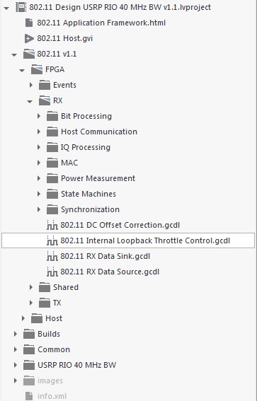
- As shown in Figure 6, find “802.11 Internal Loopback Throttle Control.gcdl” by navigating to the <project director>\802.11\FPGA\RX folder in the Navigation Pane.

Figure 6: Navigation Pane Folder Path
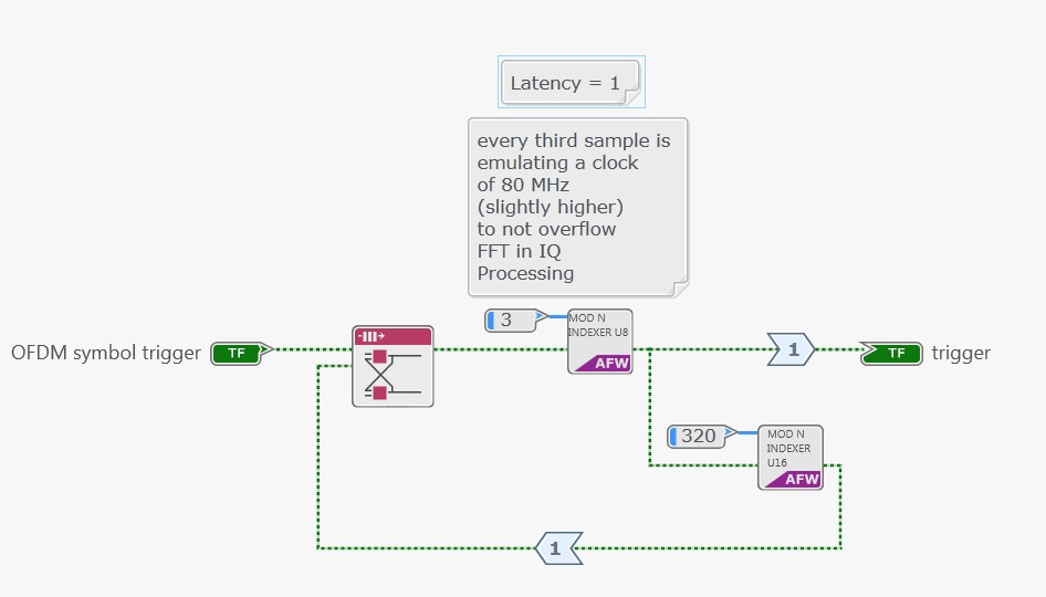
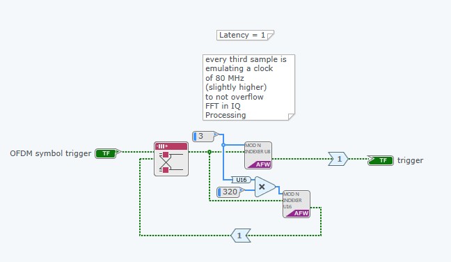
- Figure 7 shows the original, unmodified, code. Notice that the connection of the two Mod N Indexers in series together leads to a very long combinatorial path. To address this, it needs to be broken into two separate paths as shown in Figure 8.

Figure 7: Unmodified "802.11 Internal Loopback Throttle Control.gcdl"

Figure 8: Adaptation of "802.11 Internal Loopback Throttle Control.gcdl"
Migrate to the New USRP Interface
Scope
Because the USRP interface (40 MHz BW) is deprecated with LabVIEW Communications 2.0, which was used in the 802.11 Application Framework v1.1, a new interface must now be used on the FPGA toplevel. The new interface now handles both the 40 MHz BW and 120 MHz BW USRP models with the same interface. Hence, an FPGA bitfile rebuild is required.
Without the rebuild, Error -61206 will occur when running the Host top-level “802.11 Host.gvi“ as shown in Figure 9.
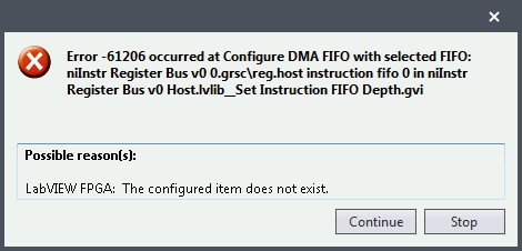
Figure 9: Error -61206 occurs when running the Host Top-level without migrating the USRP interface
Which Files are Affected?
- The FPGA top-level “802.11 FPGA STA.gvi“
Note: Two new USRP interface files must be included in the project: “Create Resources.gvi“,
“Registers.gcdl“
Step-By-Step Instructions
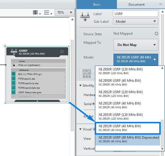
- Select your USRP Target on the System Designer and change the "Model" in the right-hand rail to the non-deprecated version (ex: NI 2953R USRP (40 MHz BW) Deprecated » NI 2953R USRP (40 MHz BW)) like in Figure 10.

Figure 10: Change Deprecated Version
- Generate a new 40 MHz Single-Device Streaming project in LabVIEW Communications 2.0 by
navigating to New » Project Templates » USRP RIO 40 MHz BW Single-Device Streaming.
Note: This project will only be used to copy the necessary project files, and code sections, into the
previous project that is being migrated.
- Copy two VIs from the new project into the original project. Refer to Figure 11.
a. Find the following subVIs from the <project directory>\FPGA subVIs folder:
i. Create Resources.gvi
ii. Registers.gcdl

Figure 11: Snapshot of Required Files
b. Copy these on disk and paste to the same directory in the original project.
c. In the “Project Files” view on the Navigation Pane of the original project, the new files will
appear slightly grayed out. Right-click on each and select Include as shown in Figure 12.
d. Since the “Create Resources.gvi” is not a specific FPGA document (for example, CDL, MRD,
and so on), there may be a prompt to select the target that the file should reside under. Select
the same USRP target that your other files in this directory reside under.

Figure 12: How to Include Additional Files in Project
- In the original project to be migrated, open the FPGA top-level “802.11 FPGA STA.gvi“
Note: If you finished all of the instructions of the first section, Reconfigure the Xilinx IP, then no error
should be displayed for the FPGA top-level.
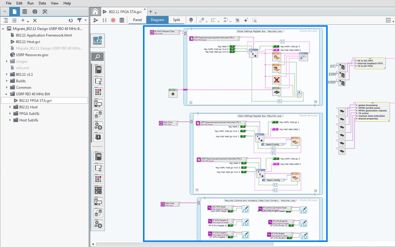
- Find the three Clock-Driven Loops used for interfacing with the USRP and remove those loops as
shown in Figure 13.

Figure 13: Deleting the Clock-Driven Loops for interfacing with the USRP
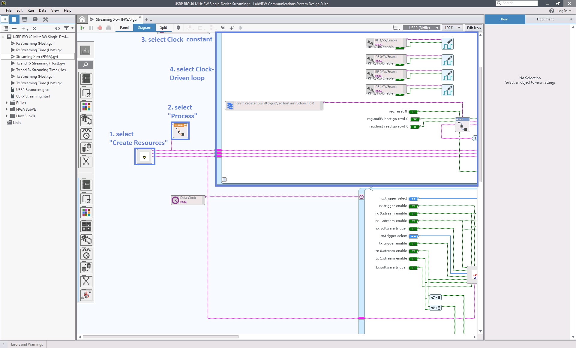
- Open the “Streaming Xcvr (FPGA).gvi” of the new project.
a. As shown in Figure 14, select and copy the following from the Diagram: “Create Resources.gvi”,
“Process.gvi”, the Clock Constant, and the Clock-Driven Loop.

Figure 14: USRP Interface Elements to be copied to the FPGA Top-Level
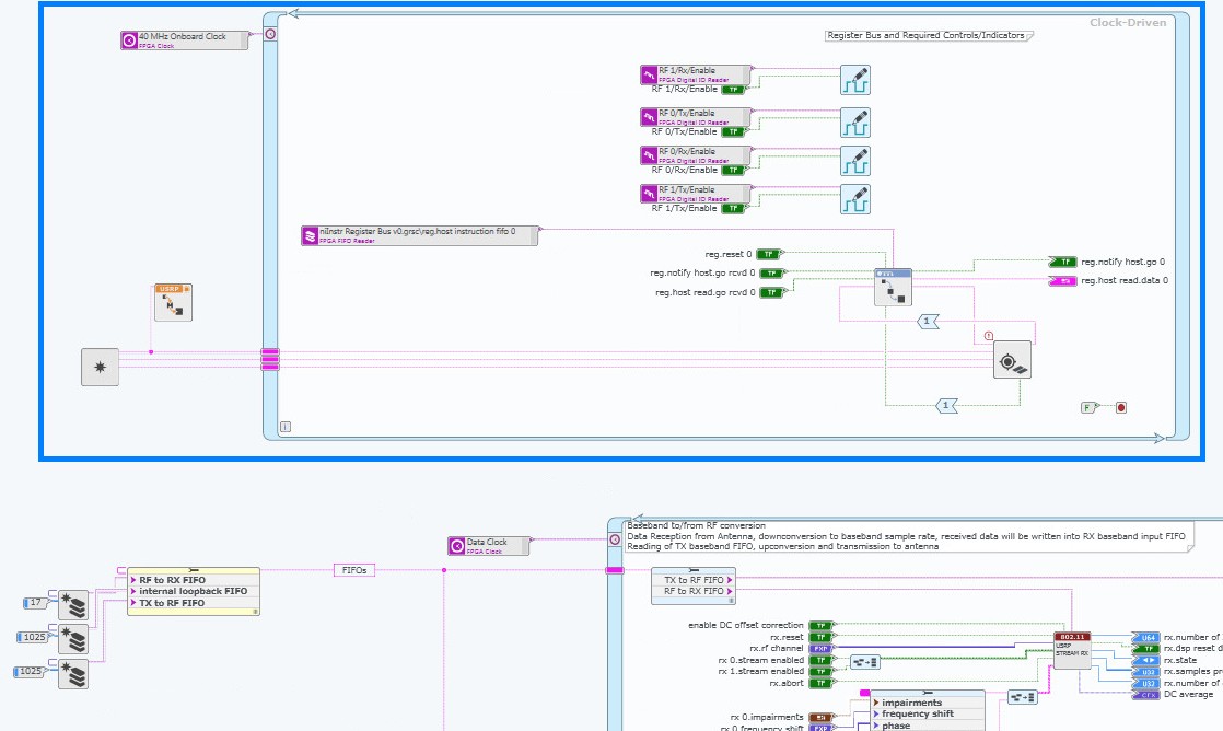
- In the project you wish to migrate, paste the elements you copied from the new streaming project
and wire as shown in Figure 15.

Figure 15: Pasted USRP interface elements wired up
- Allow all document changes to finish loading and save all files.
- Close the new streaming project as it is no longer needed.
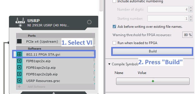
- Compile the FPGA VI.
a. Open the System Designer (in the “Project Files” view of the Navigation Pane on the left) and
double-click on the top most project file.
b. Select the FPGA top-level under the target you want to build the bitfile for.
c. Click Build on the right-hand rail as shown in Figure 16.

Figure 16: Build a bitfile for the selected FPGA Top-Level VI
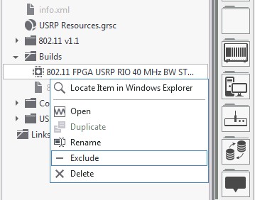
- (Recommended) Once the bitfile is finished building, exclude it from the project as shown in Figure
17 and include it again. This will ensure that the latest changes are actually applied.

Figure 17: Exclude and include the FPGA Top-Level again to make sure it is loaded correctly
Update Host-Side DMA FIFO’S
Scope
The FIFO resource names in the Host subVIs which interface with DMA FIFOs must be updated.
In LabVIEW Communications 1.0/1.1, the FIFO name contained only the name itself, for example, “T2H
Events”. In LabVIEW Communications 2.0, the FIFO resource contains additional prefixes for the FPGA
resource file name along with the FIFO name itself, for example “USRP Resources.grsc\T2H Events“.
Therefore, all occurrences of “Configure DMA FIFO“, “Read DMA FIFO“ and “Write DMA FIFO“ must
be updated to reference the new name.
Which Files are Affected?
- All Host subVIs which contain a FIFO node, for example, Start/Stop, Configure, or Read/Write
operations
The list of VIs which require modification for “802.11 Host.gvi” is included in Table 1. If you miss one
occurrence of a DMA FIFO operation, you will receive error -61206 during run-time as shown in Figure
18. In this example, the error indicates that the FIFO resource name of the node “Configure DMA FIFO“
is incorrect in the file “LTE DL RX FIFO Initialization.gvi.“
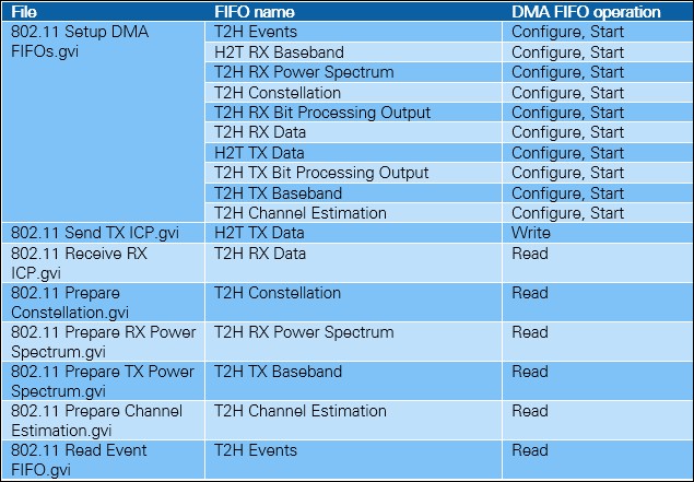
Table 1: FIFO Operations in "802.11 Host.gvi"
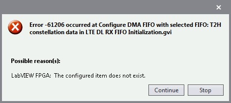
Figure 18: Error -61206 occurred because of incorrect FIFO resource name
Step-By-Step Instructions
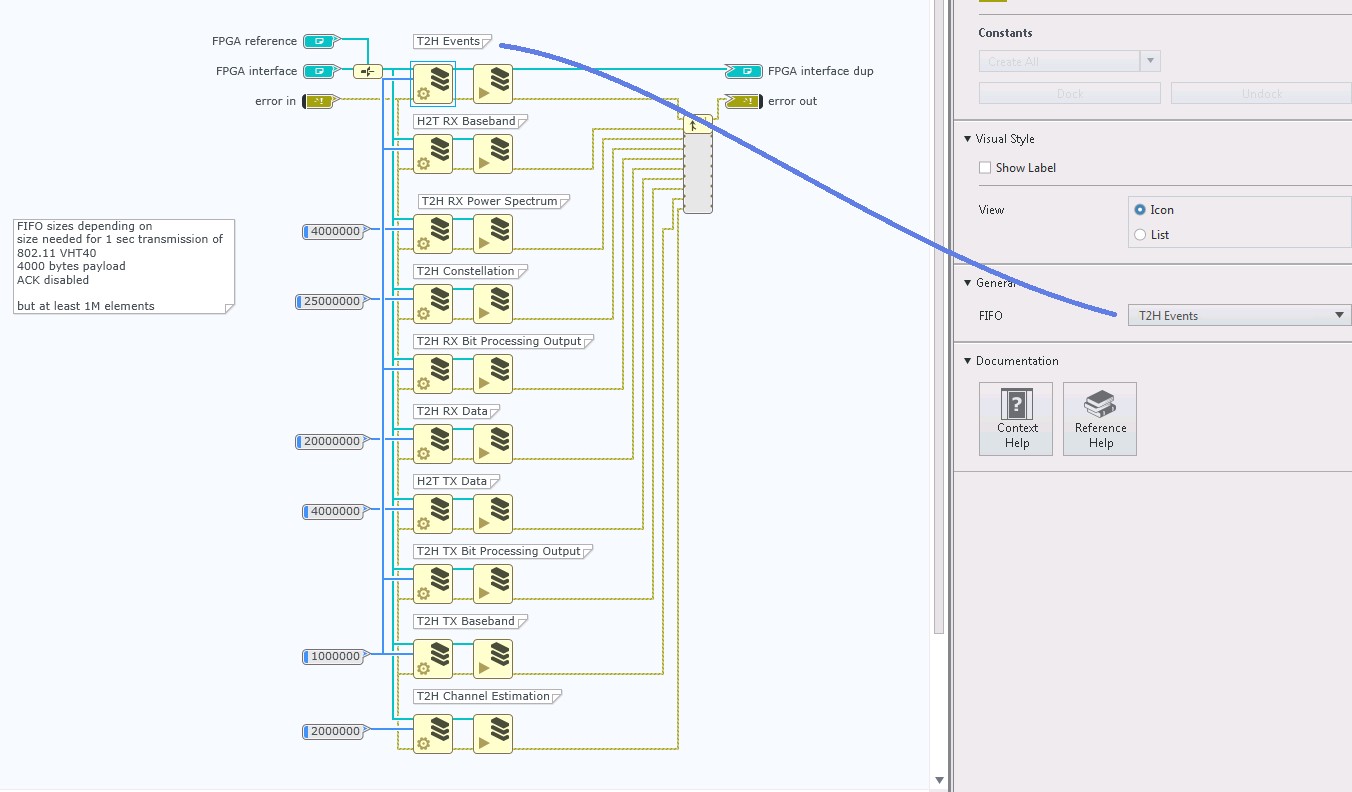
- Open the affected VI. In this example, we are demonstrating changes needed for the “802.11 Setup
DMA FIFOs.gvi”. - (Recommended) Add comments above the affected nodes which note the currently configured
resource name as shown in Figure 19.

Figure 19: “802.11 Setup DMA FIFOs.gvi” (after adding FIFO name comments)
- Select the “FPGA reference“ constant and click Configure on the right-hand rail as shown in Figure
20.

Figure 20: “802.11 Setup DMA FIFOs.gvi” - Reconfigure FPGA type
- In the “FPGA Interface Dynamic Refnum Configuration“ dialog, click Import bitfile and navigate to
the bitfile you just built in the last step of the third section, Migrate to the New USRP Interface.
- (Optional) With the “FPGA Interface Dynamic Refnum Configuration“ dialog still open, remove all
unused resources by clicking the X symbol on the right side. This will not affect functionality but may
make it easier to view used resources at a later time.
- Click OK in the “FPGA Interface Dynamic Refnum“ dialog.
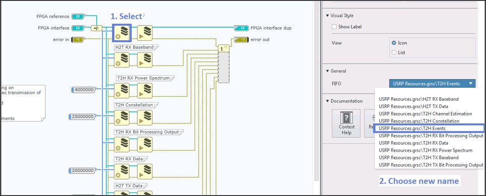
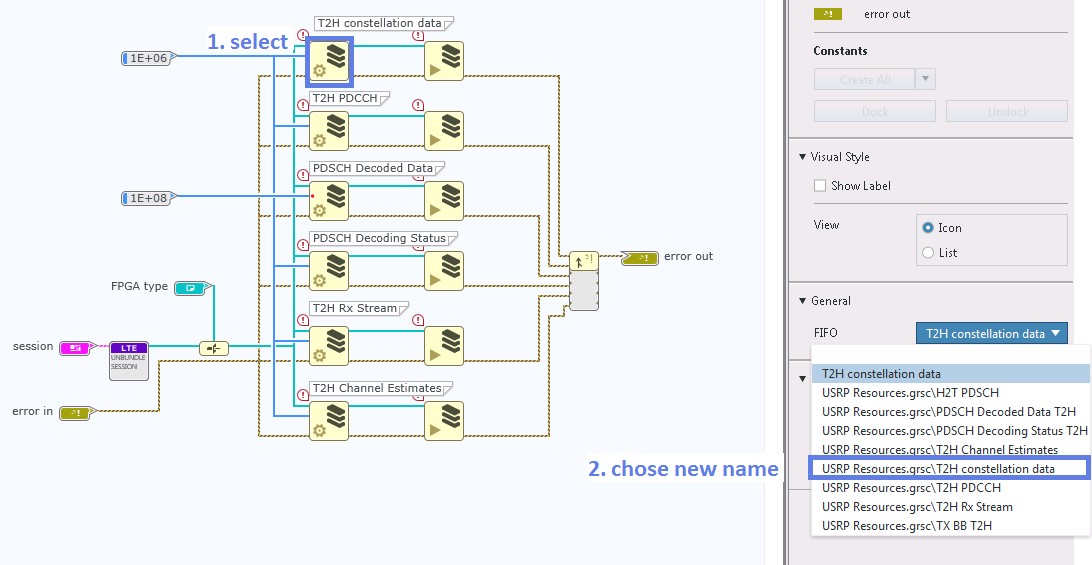
- Select the first FIFO node and adopt the FIFO name as shown in Figure 21.

Figure 21: “802.11 Setup DMA FIFOs.gvi” - Adopt FIFO Name
- Repeat the previous step for all FIFO nodes in the current VI.
Caution: Make sure to select the correct FIFO. Double-check if the name you selected matches the
comment you added to the document in step 2.
- Repeat steps 1-8 for all VIs which contain a DMA FIFO node.
Step-By-Step Instructions
- Select your USRP Target on the System Designer and change the "Model" in the right-hand rail to the non-deprecated version (ex: NI 2953R USRP (40 MHz BW) Deprecated » NI 2953R USRP (40 MHz BW)).

Figure 28: Change Deprecated Version
- Generate a new 40 MHz Single-Device Streaming project in LabVIEW Communications 2.0 by navigating to New » Project Templates » USRP RIO 40 MHz BW Single-Device Streaming.
Note: This project will only be used to copy the necessary project files, and code sections, into the previous project that is being migrated.
- Copy two VIs from the new project must be copied into the original project as shown in Figure 29.
a. Find the following subVIs from the <project directory>\FPGA subVIs folder:
i. Create Resources.gvi
ii. Registers.gcdl

Figure 29: Files to Copy
b. Copy these on disk and paste to the <project directory>\USRP RIO 40 MHz BW\FPGA directory in the original project.
c. In the “Project Files” view on the Navigation Pane of the original project, the new files will appear slightly grayed out. Right-click on each and select Include, as shown in Figure 30.
d. Since the “Create Resources.gvi” is not a specific FPGA document (for example, CDL, MRD, and so on), there may be a prompt to select the target that the file should reside under. Select the same USRP target that your other files in this directory reside under.
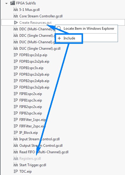
Figure 30: Include Copied Files
- In the original project to be migrated, open the FPGA top-level “LTE FPGA USRP RIO 40 MHz BW DL.gvi“.
Note: If you finished all of the instructions of the first section, Reconfigure the Xilinx IP, no error should be displayed for the FPGA top-level.
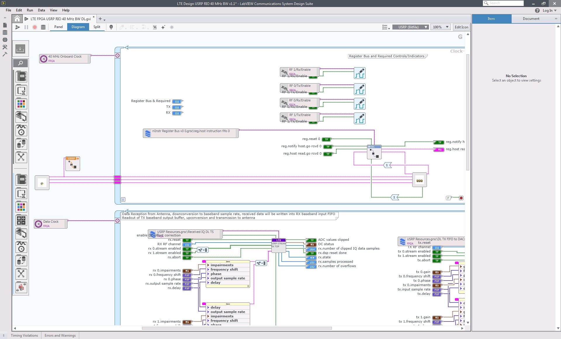
- Find the three Clock-Driven Loops which are used for interfacing with the USRP as shown in the following Figure 31.
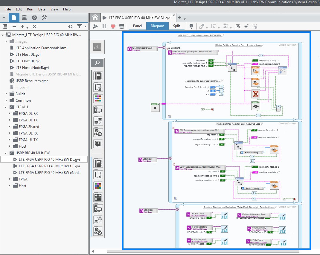
Figure 31: CDLs noted in Step 7
- Move the controls “Register Bus & Required“, “TX“ and “RX“ outside the first USRP Clock-Driven Loop as shown in Figure 32.
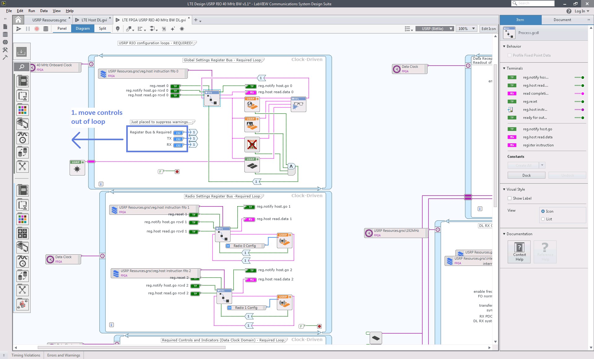
Figure 32: Clock-Driven Loops for interfacing with the USRP on the FPGA Top-Level
- Delete the three Clock-Driven Loops used for interfacing with the USRP as shown in Figure 33.
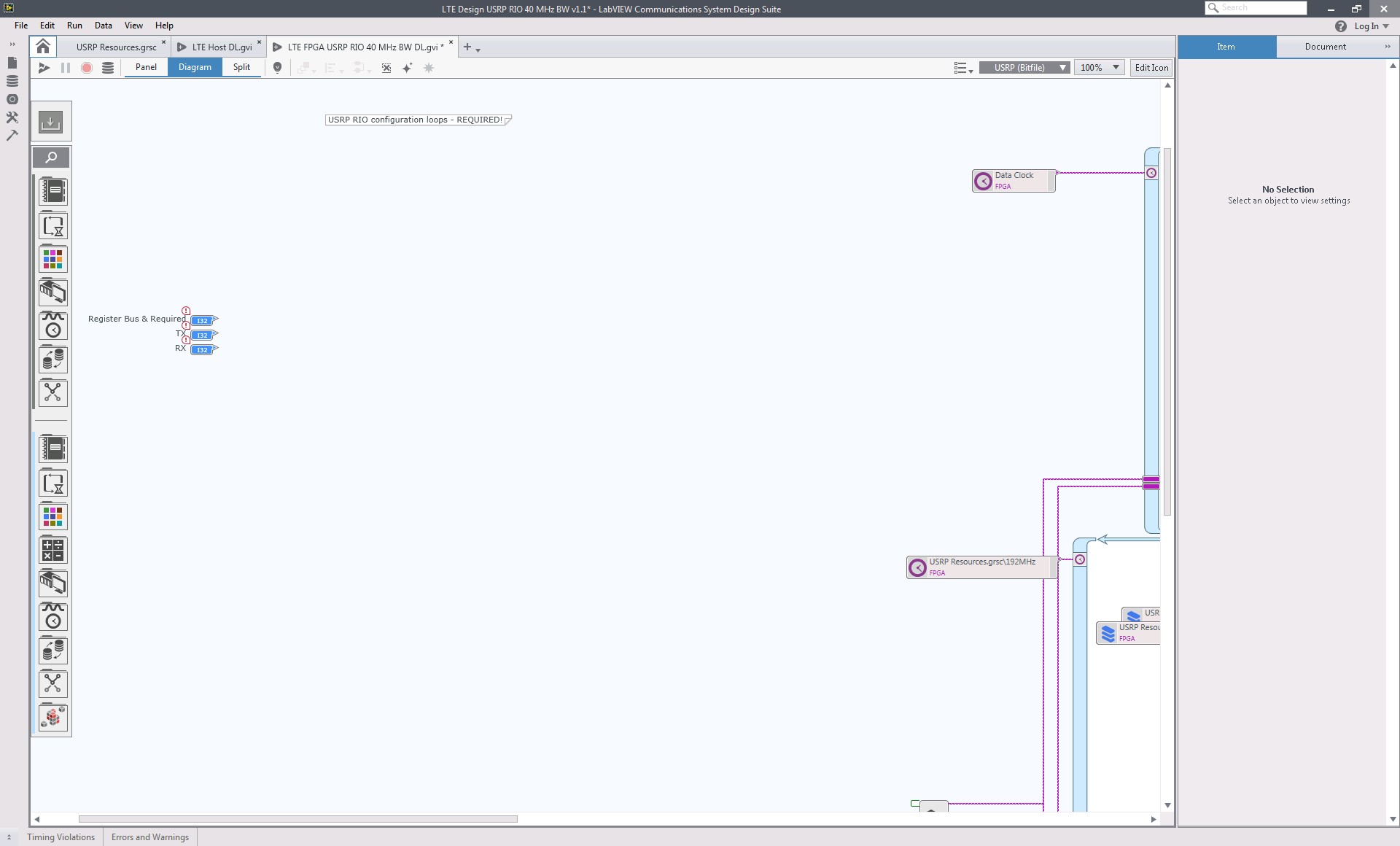
Figure 33: Deleting the Clock-Driven Loops for interfacing with the USRP
- Open the “Streaming Xcvr (FPGA).gvi” of the new project.
As shown in Figure 34, select and copy the following from the Diagram: “Create Resources.gvi”, “Process.gvi”, the Clock Constant, and the Clock-Driven Loop.

Figure 34: USRP Interface Elements to be copied to the FPGA Top-Level
- In the project you wish to migrate, paste the elements you copied from the new streaming project and wire as shown in Figure 35.

Figure 35: Pasted USRP interface elements wired up
- Allow all document changes to finish loading and save all files.
- Close the new streaming project as it is no longer needed.
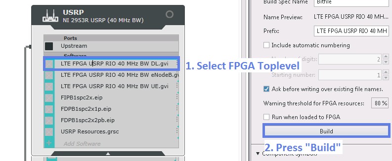
- Compile the FPGA VI.
a. Open the System Designer (in the “Project Files” view of the Navigation Pane on the left) and double-click on the top most project file.
b. Select the FPGA top-level under the target you want to build the bitfile for.
c. Click Build on the right-hand rail as shown in Figure 36.

Figure 36: Build a bitfile for the selected FPGA Top-Level VI
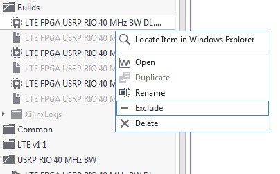
- (Recommended) Once the bitfile is finished building, exclude it from the project as shown in Figure 37 and include it again. This will ensure that the latest changes are actually applied.

Figure 37: Exclude and include the FPGA Top-Level again to make sure it is loaded correctly
Update Host-Side DMA FIFO’S
Scope
The FIFO resource names in the Host subVIs which interface with DMA FIFOs must be updated.
In LabVIEW Communications 1.0/1.1, the FIFO name contained only the name itself, for example, “PDSCH Decoding Status“. In LabVIEW Communications 2.0, the FIFO resource contains of the prefixes the FPGA resource file name and the FIFO name itself, for example, “USRP Resources.grsc\PDSCH Decoding Status“.
Therefore, all occurrences of “Configure DMA FIFO“, “Read DMA FIFO“ and “Write DMA FIFO“ must be updated to reference the new name.
Which Files are Affected?
- All Host subVIs which contain a FIFO node (for example, Start/Stop, Configure, or Read/Write operations)
The list of VIs which require modification for “LTE Host DL.gvi” is included in Table 2. If you miss one occurrence of a DMA FIFO operation, you will receive error -61206 during run-time as shown in Figure 38 in which the error indicates that the FIFO resource name of the node “Configure DMA FIFO“ is incorrect in the file “LTE DL RX FIFO Initialization.gvi.“
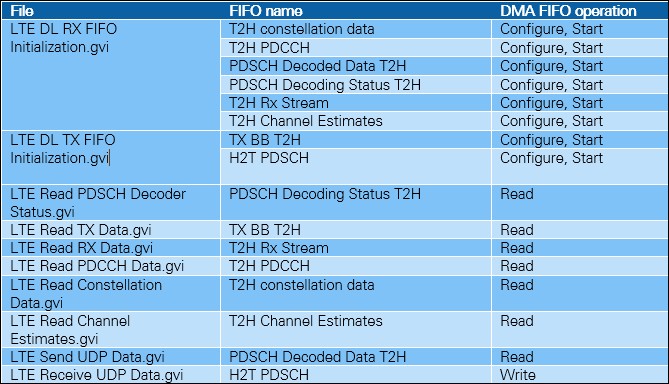
Table 2: FIFO “Operations in LTE Host DL.gvi”

Figure 38: Error -61206 occurred because of incorrect FIFO resource name
Step-By-Step Instructions
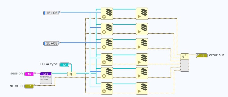
- Open the affected VI. In this example, we are demonstrating changes needed for the “LTE DL RX FIFO Initialization.gvi” as shown in Figure 39.

Figure 39: “LTE DL RX FIFO Initialization.gvi” (original file)
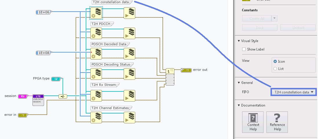
- (Recommended) Add comments above the affected nodes that note the currently configured resource name as shown in Figure 40.

Figure 40: “LTE DL RX FIFO Initialization.gvi” (after adding FIFO name comments)
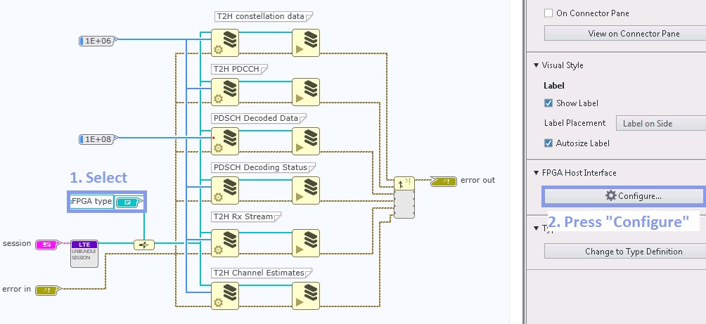
- Select the “FPGA type“ constant and click Configure in the right-hand rail as shown in Figure 41.

Figure 41: “LTE DL RX FIFO Initialization.gvi” - Reconfigure FPGA Type
- In the “FPGA Interface Dynamic Refnum Configuration“ dialog, click Import bitfile and navigate to the bitfile you just built in the last step of the second section, Migrate to the New USRP Interface.
- (Optional) With the “FPGA Interface Dynamic Refnum Configuration“ dialog still open, remove all unused resources by clicking the X symbol on the right side. This will not affect functionality but may make it easier to view used resources at a later time.
- Click OK in the “FPGA Interface Dynamic Refnum“ dialog.
- Select the first FIFO node and adopt the FIFO name as shown in Figure 42.

Figure 42: “LTE DL RX FIFO Initialization.gvi” - Adopt FIFO name
- Repeat the previous step for all FIFO nodes in the current VI.
Caution: Make sure to select the correct FIFO. Double-check if the name you selected matches the comment you added to the document in step 2.
- Repeat steps 1 through 8 for all VIs which contain a DMA FIFO node
