Switching Low-Level Signals to a DMM
Overview
Many high resolution digital multimeters (DMM) today have the ability to measure extremely low-level signals. For instance, the NI PXIe-4081 DMM is a 7½ digit DMM with the ability to measure in the nanovolt, picoamp, and micro-ohm range. Concerns often arise that using switching in front of the DMM will decrease its ability to make these low-level measurements. This document will describe the fundamental principles that affect low-level measurements, which relay types best address these principles, the recommended NI Switches to use, and other tips and techniques for making low-level measurements.
Contents
General Considerations for All Signals
For all types of low-level measurements there are some techniques that should be employed:
- Use shielded cables of high-resistance insulation. The insulation should preferably be a non-moisture absorbing material such as Teflon.
- All measurements should be taken after the equipment (DMM and switches) have warmed up for at least 15 minutes. After which, ensure that the ambient temperature does not change appreciably, if possible within 1°C.
- Use software filtering and noise reduction techniques. Often, a constant offset can be measured and calibrated out of the measurement in software. If extremely low signals are being measured then the measurements should be calibrated per path. Additionally, increasing the measurement aperture of your DMM will increase the measurement averaging that takes place and give you a more accurate reading.
- Keep cables and leads from potential sources of electromagnetic interference, such as power outlets.
Low Voltage
The primary consideration for low voltage measurements is the Thermal EMF or Offset Voltage associated with the relay.
Thermal EMF
When two, dissimilar metals are joined a voltage is created. This voltage is known as the thermal electromotive force (EMF) or the Seebeck voltage. The Seebeck voltage is dependent on the temperature of the junction and the composition of the metals joined. The specific metal-to-metal junctions result in specific temperature coefficients (µV/°C), also known as Seebeck coefficients. The following table lists the most common metals and their respective Seebeck coefficients.
| Junction | µV/°C | |
| <0.3 | |
| 0.5 | |
| Copper-Silver | 0.5 | |
| Copper-Brass | 3 | |
| Copper-Nickel | 0.5 | |
| Copper-Lead-Tin Solder | 1-3 | |
| Copper-Aluminum | 5 | |
| Copper-Kovar | 40 | |
| Copper-Copper Oxide | >500 |
Thermal EMF in switches
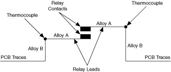
The leads of electromechanical relays are usually composed of metal alloys, most often nickel-iron alloy, while the PCB of a switch module is usually composed of copper or copper alloy. The junction between these two, dissimilar metals creates a thermocouple, as illustrated in the figure below.
| Note A thermocouple developed in a relay is dependent on the temperature of the junction. The temperature of a junction varies according to the ambient temperature, the number of relays activated, the air flow inside the switch module, and the types of switch modules located in the adjacent slots. |
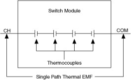
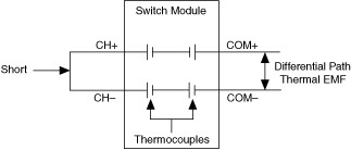
A signal path can transverse a single relay or multiple relays. The sum of all the thermocouples in a signal path is expressed as the thermal EMF. Thermal EMF can be specified as single path (single wire) or differential path thermal EMF. The figure below illustrates thermal EMF measured in a single path.
The figure below illustrates thermal EMF measured in a differential path.
See "Other Low Voltage Tips and Techniques" below for minimizing Thermal EMF.
Offset Voltage
The discussion above applies to electromechanical armature and reed relays. FET and SSR switches do not have a thermal EMF in the same sense as reed and armature relays. They do, however, have an offset voltage due to the heating of transistors in the relay circuitry. This offset voltage is comparable to the thermal EMF of armature and reed relays and is expressed in the same units, thus we can compare thermal offset between all four relay types.
Thermal EMF or offset voltage ratings are given for the entire switch module. For instance, the NI PXI-2503 has a thermal EMF of <2 µV. This is not the thermal EMF for each relay in the switch module, but rather for the module as a whole. Additionally, this value is also taken as a worse-case scenario estimate being that the signal path may go through a variable amount of relays depending on the topology of the switch and the channel chosen.
An Additional Note on Accuracy
When measuring voltage with a switch and a DMM, be sure to account for thermal EMF in the overall system accuracy calculation.
For example, if the DMM has an accuracy of 4 µV and the switch has a differential path thermal EMF of 3 µV, the overall system accuracy can be calculated as follows: √(4² + 3³) = 5 µV
Thus, when measuring a 50 mV signal, the overall system accuracy is 0.01%.
Which Relays to Use for Low Voltage?
Electromechanical armature relays have a thermal offset that is comparitively low and can range from <1 µV to around 10 µV. For instance, the NI PXI-2503 armature switch has a thermal offset of <2 µV. Additionally, latching relays are preferred to non-latching relays because the lack of coil heating minimizes EMF which can affect your measurements.
Reed relays traditionally have a higher thermal EMF: from around 5 µV to well over 50 µV. This is due to the ferromagnetic materials from which reed relays are constructed. For instance, the NI PXI-2530B reed switch has a thermal offset of 50 µV.
FET relays have a thermal offset closer to electromechanical armature. For instance, the NI PXI-2501 FET switch has a thermal offset of 2.5 µV.
SSR relays have a higher thermal offset than either electromechanical armature or FET switches. For instance, the SCXI-1128 SSR switch has an offset voltage of <25 µV from 0 °C to 25 °C.
Top Low Voltage Picks
PXI-2501 multiplexer/matrix, PXI-2503 multiplexer/matrix, PXI-2527 multiplexer
All switches listed above have a low thermal offset and are excellent choices for low voltage measurements. The PXI-2501 has the added benefit of extremely fast switching: the relay scan rate is 15,000 cycles/s as compared to 100 operations/s with the electromechanical armature relays (PXI-2503, PXI-2527). However, the thermal offset for the armature relays is slightly lower in general than that for the FET switches.
Other Low Voltage Tips and Techniques
A common technique used in metrology labs for very accurate measurements is to take a measurement, switch the leads, repeat, subtract and average the readings.
Thermal EMF will always exist in connections, but by remembering that it is temperature dependent, error can be minimized. If the connections do not change temperatures, then the thermal voltage is stable and can be corrected; it is temperature changes between these junctions that create problems (such as offset drift, instability, and very low frequency noise). The key to preventing changes in temperature is to prevent circulating air currents that can disturb the thermal equilibrium of the junctions. This leads to another rule for low-voltage measurements: keep junctions and connections at a stable temperature and away from circulating air currents caused by movement, fans, and so on. These temperature differences can be prevented by creating a "thermal baffle," such as wrapping the junctions with common foam padding (even Styrofoam sheet can work) and keeping them away from sources of heat such as equipment heat sinks and sunlight.
When copper oxidizes, the Seebeck coefficient can easily increase by several hundred µV/°C. This leads to another rule for low-voltage measurements: keep the connections clean. One option is to simply use a pencil eraser to clean the bare wire until the wire is shiny, then clean off any rubber fragments with a paper towel. Another way to clean connections is to use Scotchbrite pads to clean the wire. After cleaning the connections, connections should not be handled with the fingers. Skin oil contains a very effective corrosive that accelerates oxidation of many metals.
Low Current
Minimum Current Required for Burn-off
Another concern is the current required to burn off very small particles on the contacts of armature relays. When relays are in their open position, small particles can accumulate on the contacts for the closed position. When contact is made, a minimum amount of current is needed to burn off these particles and establish the connection. For smaller relays this amount is in the mA range. For relays with a higher maximum current rating, the contacts are larger and thus a greater area is available for particle deposition and a greater amount of current is required to burn off these particles. Reed relays are not subject to this problem because the contacts are encapsulated in a noble gas.
Top Low Current Picks
PXI-2530B multiplexer/matrix, PXI-2532 matrix
The above switch models are excellent picks due to the fact that they use reed relays.
Other Low Current Tips and Techniques
Low-level measurements are susceptible to sources of error and noise that are often negligible for higher level measurements. In the low-level signals world, no material is an ideal insulator. Some materials are better insulators than others. Selection of proper cables and interconnects becomes very important.
When making low-level current measurements, noise and error sources are more likely to affect measurements in the order of 10µA or less. Take into account the recommendations listed in the table below to ensure measurement integrity.
Error or Noise Source
| Cause
| Level of Induced Error
| Recommendations
|
| Input bias current |
| Typically 10 pA at 23 °C ambient, but it is factory calibrated to zero at that temperature. |
|
| Leakage currents due to poor insulation | When measuring low-level currents, leakage currents in insulators become relevant. Current flows between a high-impedance point and the nearby voltage sources. | Depends upon the resistivity of the insulator material. Some examples include the following:
| Be sure that the test fixture for the DUT is constructed of a material appropriate for the desired test and that the test fixture is clean. |
| Noise currents due to triboelectrics1 | Currents are generated by moving the cables because a transfer of charge occurs between the insulator and the conductor when they rub against each other. | Hundreds of pA in a polyethylene cable (for example, RG-58) |
|
| Noise currents due to piezoelectrics2 | Currents can be generated when the insulator is subjected to mechanical stress. | Hundreds of pA for polyethylene |
|
| Error currents due to contamination and humidity | Insulation resistance gets reduced with increasing humidity and contamination. These two combined could also generate small electrochemically-induced currents. | On the order of pA to µA |
|
| Noise currents due to electromagnetic interference and electric fields | Surrounding equipment (motors, power cables, vibrating equipment) can induce noise currents. Moving people and charged objects near measurement setup can induce electrostatic coupling. | On the order of nA and tens of µA depending on proximity, device shielding, and magnitude of relative movement |
|
| Burden voltage | Refer to the Burden Voltage section below | Depends on the circuit being measured | Calculate if the error caused by burden voltage is relevant when measuring the current in the circuit of interest. Refer to the Burden Voltage section below for an example. |
| Leakage currents due to external switching | External switches used for routing low level currents could be a source of leakage currents. | Depends on the switch, temperature and humidity of the environment. |
|
| 1The Triboelectric Effect can be compared to the phenomenon of static electricity caused by rubbing certain insulators together. Teflon and silver in combination, for example, can create a very high level of triboelectric-induced current noise. 2The Piezoelectric Effect, although well-exploited in sensors which convert changes in pressure from sound waves or physical vibration into small voltage signals, is highly undesirable in cables and interconnects. |
Burden Voltage
Burden voltage is the voltage drop caused by current flowing through a current measuring device. A large burden voltage can affect the circuit being measured, corrupting the measurement. For this reason, it is desirable for burden voltage to be kept as low as possible.
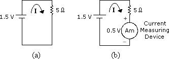
The following figure shows a 1.5 V source with a 5 Ω load. To measure the current on the circuit, an ammeter is connected in series with the circuit. In this figure, the ammeter has a 0.5 V burden voltage.
Without burden voltage (figure a), the calculated current is:
Iactual = 1.5 V / 5 Ω
Iactual = 0.3 A
With burden voltage (figure b), the current in this circuit equals:
Imeasured = (1.5 V-0.5 V ) / (5 Ω)
Imeasured = 0.2 A
In the figure above, burden voltage of the current measuring device subtracts from the voltage across the 5 Ω resistor. The result is a significant error in the measurement. In this case, the error caused by the burden voltage is 33%. Problems like this can easily crop up when using a shunt resistor to measure the current drawn by logic voltages <3.3 V common in today's digital systems.
For the maximum burden voltage per range, refer to the specifications documents for the DMM being used.
Possible techniques to reduce error caused by ammeter burden voltage include the following:
- When using the current function within the DMM, keep leads to the switch short and use the appropriate gauge of cable to minimize voltage drops from leads.
- Sense remotely with external shunts to eliminate the need for long current-carrying cables to the switch and DMM. Use the lowest value of shunt resistance that the measurement allows.
- Use wires in the circuit under test as resistance shunts. Measure the voltage drop across the wire. Then, use the Offset Compensated Ohms feature to measure the resistance of the wire, and calculate I = Vwire/Roco.
Low Resistance
Path Resistance
Path resistance is again a major concern when switching low resistance signals. Path resistances can be calibrated out of measurements in software but allowing switches with larger path resistances will require a larger gain and/or range with the DMM used which will decrease the resolution with which the measurement is taken. Refer to the Path Resistance section under Low Current above for more information.
4-Wire Mode
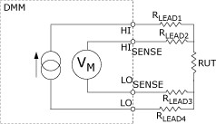
For precision measurements with resistances below 100 kΩ, the 4-wire mode is more accurate than the 2-wire mode. The 4-wire mode requires 4-wire switching and more cabling; however, for very low voltages it is highly recommended.
The following figure shows a 4-wire resistance measurement, including lead resistance:
In 4-wire resistance measurements, current is forced through the source terminals (HI, LO). The sense terminals (HISENSE, LOSENSE) are configured for very high impedance, and this configuration directs current through the resistance under test (RUT). As a result, voltage develops across RUT as well as across RLEAD1 and RLEAD4. By measuring the voltage directly across RUT using the sense leads (RLEAD2, RLEAD3), the voltage drop of the source leads (RLEAD1, RLEAD4) is removed from the measurement path.
Offset Compensated Ohms
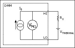
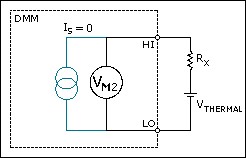
Thermal EMF and offset voltage is only a factor if the measurement is taken without Offset Compensated Ohms (OCO). Offset Compensated Ohms is a DMM feature provided for eliminating offset voltages in a resistance test system. The measurement involves two cycles as shown in the following figures. The first figure represents the first cycle with the current source ON:
The second figure represents the second cycle with the current source OFF:
The net result is the difference between the two measurements. Because the offset voltage is present in both cycles, it is subtracted out and does not affect the resistance calculation.
Which Relays to Use?
Electromechanical armature and reed relays are both excellent choices for low resistance measurements because of their low path resistance. For instance the PXI-2503 armature switch has a path resistance of <1 Ω and the PXI-2530B reed switch has a path resistance of <2 Ω. FET and SSR switches are not recommended due to a path resistance that is generally in the kΩ range.
Top Low Resistance Picks
The PXI-2503 multiplexer/matrix armature switch has an extremely low path resistance. If greater speed is needed, the PXI-2532 matrix and PXI-2530B multiplexer/matrix multiplexer/matrix reed switches offer faster switching speeds.
Summary
FET switches and electromechanical armature switches are an excellent solution to low-voltage switching needs due to their low voltage offset. The PXI-2501/2503/2527 are specifically recommended.
Reed switches are the best solution for low-current switching needs due to their low path resistance and lack of minimum switching current. The PXI-2530B/2532 and are all excellent choices.
Electromechanical armature and reed switches are excellent for switching low-resistance signals due to their low path resistance. The PXI-2503/2532/2530B are the top picks.
