An Introduction to PXI High-Speed Serial Instruments
Overview
PXI High-Speed Serial Instruments help engineers validate, interface through, and test high-speed serial protocols. Select high-speed serial devices, such as the PXIe-7903 and PXIe-7902, were designed for engineers who need high-performance FPGA coprocessing capabilities to achieve high-volume data movement and inline real-time signal processing. This hardware has a Xilinx Kintex™ UltraScale+™ or 7 series FPGA, which you can program with the LabVIEW FPGA Module for maximum application-specific customization and reuse. These instruments take advantage of FPGA multigigabit transceivers (MGTs) to support line rates up to 28.2 Gbps and up to 48 TX and RX lanes. As part of the PXI platform, they benefit from PXI clocking, triggering, and high-speed data movement capabilities, including streaming to and from disk, as well as peer-to-peer (P2P) streaming at rates up to 7 GB/s.
Contents
- The Emergence of High-Speed Serial Interfaces
- High-Speed Serial Modules
- Example Applications
- Skills Required
- Next Steps
The Emergence of High-Speed Serial Interfaces
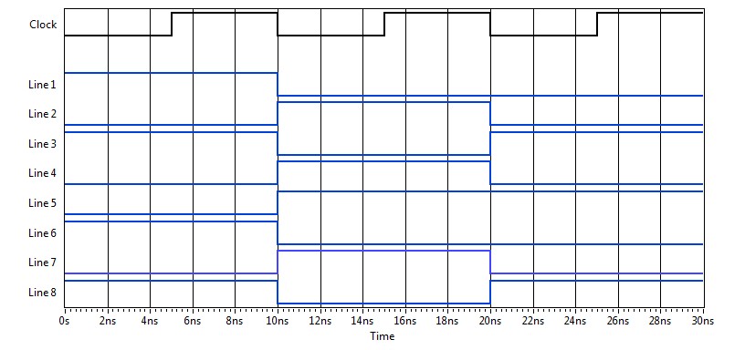
With the ever-increasing demand for higher data bandwidth, wired interfaces have increased their clock rates and parallelism to keep up. However, with traditional parallel data buses, the smallest amount of skew between the clock and data lines can threaten the bit error rate of the interface. Serial data links offer a solution to this issue by embedding the clock into the data stream of a given pair of differential traces, which eliminates the possibility of skew between the clock and the data. This feature requires additional electronics at the receiving end of the interface as well as additional encoding for clock recovery; however, it makes dramatically higher data rates possible, which satisfies the demand for bandwidth.
Figure 1. Parallel clock (black) and data (blue) versus embedded clock in data (red), with equivalent data bandwidth.
Modern data communication protocols have transitioned from these parallel interfaces to high-speed serial interfaces, such as PCI Express, HDMI and DisplayPort video standards, IEEE 1394b, USB 3.0, and more. For design and test engineers, validating these interfaces presents new challenges that require new test hardware. Traditionally, engineers have used expensive oscilloscopes or bit error rate testers (BERTs) to characterize the physical interfaces and have used protocol-specific analyzers and generators to validate that the protocol stack is implemented correctly, and that data transmission and reception operate efficiently. For automated V&V and manufacturing test, however, optimized hardware to test these serial interfaces doesn’t exist. Oscilloscopes and bit error rate testers are often too expensive and slow to justify the coverage they provide, while protocol-specific hardware is often not flexible enough to integrate into automated test systems. Protocol-specific hardware, on the other hand, cannot be reused for other tests or repurposed for other devices under test (DUTs).
FPGAs provide a solution for these challenges. Modern, high-performance FPGAs generally include several MGTs that work with a variety of high-speed serial interfaces. When combined with the appropriate protocol-specific IP, graphical programming through the LabVIEW FPGA Module, and the advantages of the PXI ecosystem, a new high-speed serial, software-designed instrument emerges.
High-Speed Serial Modules
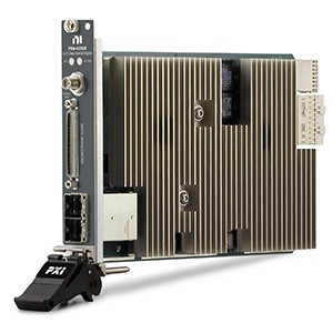 | 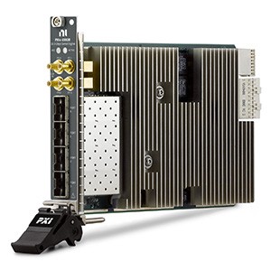 | 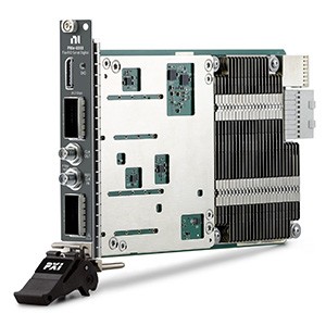 | 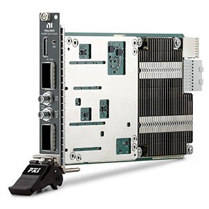 | 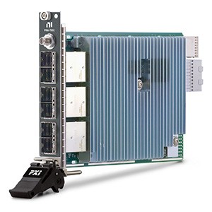 | 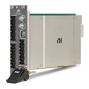 | |
| Spec | PXIe-6591 | PXIe-6592 | PXIe-6593 | PXIe-6594 | PXIe-7902 | PXIe-79032 |
| Line Rate | 500 Mbps–12.5 Gbps¹ | 500 Mbps–10.3125 Gbps¹ | 500 Mbps–16.3 Gbps | 500 Mbps–28.2 Gbps | 500 Mbps–12.5 Gbps | 500 Mbps–28.2 Gbps |
| Channels | 8 TX/RX | 4 TX/RX | 8 TX/RX | 8 TX/RX | 24 TX/RX | 48 TX/RX |
| FPGA | Kintex 7 K410T | Kintex 7 K410T | Kintex UltraScale KU040, KU060 | Kintex UltraScale+ KU15P | Virtex™ 7 485T | Virtex UltraScale+ XCVU11P |
| DRAM | 2 GB | 2 GB | 4 GB | 8 GB | 2 GB | 20 GB |
| Host Streaming BW | 3.2 GB/sec | 3.2 GB/sec | 7 GB/sec | 7 GB/sec | 3.2 GB/sec | 7 GB/sec |
| Connector | Mini-SAS HD | SFP+ | QSFP28 | QSFP28 | Mini-SAS HD | Mini-SAS HD |
| Cabling Options | Copper or Optical | Copper or Optical | Copper or Optical | Copper or Optical | Copper or Optical | Copper or Optical |
| Aux DIO | 20 SE | 4 SE | 8 GPIO | 8 GPIO | N/A | 8 GPIO |
Table 1. PXI High-Speed Serial Instruments.
¹Gap in achievable line rates between 8 Gbps and 9.8 Gbps.
²The PXIe-7903 is a 2-slot module.
Connectivity and cabling are critical with applications that have the high data rates and analog bandwidths exceeding 20 GHz. The PXIe-7903, PXIe-7902, PXIe-6594, PXIe-6593, PXIe-6592, and PXIe-6591 each provide distinct options to simplify connectivity for specific use cases. All three modules feature a user-programmable Xilinx FPGA at their core.
The Xilinx 7 Series GTX transceivers are the key technology behind these instruments. They use current mode logic (CML), which is a differential interface that features a small signal swing of 800 mVpp (nominally, 1,000 mVpp maximum) for reduced power consumption and radiated emissions, and a 100-ohm differential (50 ohm per signal leg) impedance to minimize reflections and the resulting signal aberrations at high data rates. Additionally, for optimum signal fidelity, these transceivers include a programmable transmit amplitude to compensate for long cables as well as transmit pre- and post-emphasis and auto-adaptive receiver equalization to overcome limited analog channel/cable bandwidth.
All high-speed serial interfaces require a reference clock that operates at an integer divisor of the line rate. For maximum flexibility, the GTX transceivers include a phase-locked loop (PLL) that can multiply the reference clock up to 100 times to produce the serial data rate. They also include serial-to-parallel and parallel-to-serial converters with ratios up to 80X, limiting FPGA clock frequencies while enabling high serial data rates. Furthermore, the transceivers have built-in 8b/10b, 64b/66b, and 64b/67b encoding and decoding structures to ensure a sufficient number of signal transitions for clock recovery, and to avoid consuming general-purpose FPGA resources. The Xilinx 7 Series FPGAs GTX/GTH Transceivers User Guide provides more details on Xilinx GTX transceivers.
In addition to providing high-speed serial transceivers, the Xilinx FPGAs on the instruments serve several other vital purposes. They implement the logic for the protocol in use, as well as any application-specific user logic for hardware configuration and data generation, reception, and movement throughout the system.
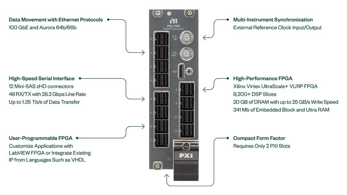
Figure 2. PXIe-7903 Hardware Architecture with Key Interfaces and Data Rate.
| Spec | FPGA | LUTs | DSP Slices | Embedded Block RAM |
| PXIe-6591 | Kintex-7 K410T | 254,200 | 1,540 | 28 Mb |
| PXIe-6592 | Kintex-7 K410T | 254,200 | 1,540 | 28 Mb |
| PXIe-6593 | Kintex UltraScale KU040 | 242,400 | 1,920 | 21.1 Mb |
| Kintex UltraScale KU060 | 331,680 | 2,760 | 38 Mb | |
| PXIe-6594 | Kintex UltraScale+ KU15P | 523,000 | 1,968 | 34.6 Mb |
| PXIe-7902 | Virtex-7 485T | 303,600 | 2,800 | 37 Mb |
| PXIe-7903 | Virtex UltraScale+ XCVU11P | 2,835,000 | 9,216 | 341 Mb |
Table 2. PXI High-Speed Serial Instruments and Their Respective FPGA Specifications.
Directly connected to the FPGAs are up to 20 GB of onboard DDR3 DRAM that can be read from or written to at rates up to 25 GB/s (theoretical maximum) in user-defined access patterns. The FPGA also includes a PCI Express x8 Gen 3 interface to the PXI Express backplane for data streaming to and from host and disk, or P2P to other FPGA-enabled devices in the system at unidirectional rates up to 7 GB/s and bidirectional rates up to 2.4 GB/s in each direction (4.8 GB/s aggregate).
A low-jitter, high-fidelity reference clock is a critical component of any high-speed serial communications system. All modules have an onboard, any-rate synthesizer for MGT operation over the full range of the Xilinx GTX transceivers, with the PXIe-6591, PXIe-6592, and PXIe-7902 operating from 500 Mbps to 8 Gbps and 9.8 Gbps to their maximum device rates, while the PXIe-6593, PXIe-6594, and PXIe-7903 operate with no such gap between their minimum and maximum line rates. The PXIe-6591, PXIe-6592, PXIe-6593, and PXIe-6594 feature front-panel coaxial connectivity for exporting the built-in reference clock, and all four modules have connectivity for importing an external reference clock. Finally, the devices can route the PXI Express 100 MHz or DStarA backplane clocks as a reference for the MGTs.
Software
A software-designed instrument provides the same functionality as a fixed-function instrument, but users can customize the instrumentation hardware through an open, user-programmable FPGA. This level of customization is necessary in a PXI High-Speed Serial Instrument to support a variety of protocols and applications. As such, there is no single high-level API for programming these devices. Instead, they are programmed directly in LabVIEW software for both the host (CPU) and FPGA code, interfacing between the two with the lower-level NI-RIO API. To help users get up and running quickly, a multitude of examples demonstrate the use of different protocols, as well as different use models for these instruments.
The open FPGA provides a degree of customization not found in other instruments. First and foremost, it implements the serial protocol for which the instrument is configured. This alone makes it possible for the PXIe-7903, PXIe-7902, PXIe-6594, PXIe-6593, PXIe-6592, and PXIe-6591 to support a multitude of standard and even custom serial protocols. Beyond just the protocol, user-defined hardware functionality allows types of tests not previously possible. For instance, algorithmic data generation on the FPGA reduces the required waveform storage memory and system bandwidth for downloading these waveforms, which accelerates test throughput. Algorithmic data analyses such as response comparison, intelligent triggering, and data reduction and compression drastically reduce the amount of data for the host CPU to process, which also decreases test time.
User-defined DRAM access allows flexibility in how the DRAM is partitioned into stimulus and response regions. It also enables custom compression and decompression algorithms, which allows for optimal use of DRAM size and bandwidth. Standard waveform capture and playback is certainly possible, but depending on the protocol, line rate, and number of lanes, I/O bandwidth may exceed DRAM bandwidth. Finally, user-defined data movement to and from a high-speed serial instrument and the host or other instruments delivers significant flexibility for system-level integration. For example, it is possible to convert analog data to digital samples with a high-speed digitizer, use NI P2P streaming to transfer that data to a high-speed serial instrument at rates up to 7 GB/s, and then transmit those digital samples to an external device over a serial protocol. Alternatively, a high-speed serial instrument can capture a serial data stream and transfer it to the host CPU and ultimately a high-bandwidth RAID array for hours or even days of continuous storage, again at rates up to 7 GB/s.
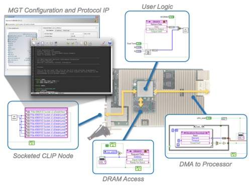
LabVIEW FPGA makes it simple to configure and program these high-speed serial instruments. Figure 3 highlights the key interfaces accessible through LabVIEW, along with representative code. LabVIEW FPGA and the NI-RIO API provide efficient mechanisms for PCI Express-based data transfer between the host CPU and the FPGA, including register reads and writes as well as bi-directional DMA transfers. DRAM access—typically a challenging interface to manage in lower-level hardware description languages (HDLs)—is simplified through abstracted request, read, and write interfaces while maintaining high throughput and providing basic read/write arbitration. GTX transceiver configuration is generally protocol-specific, and IP already exists for many high-speed serial interfaces (either HDL or netlist) with built-in transceiver configuration. This serial protocol interface is exposed in LabVIEW FPGA through a socketed component-level IP (CLIP) interface. CLIP nodes allow for the asynchronous operation of code not implemented in LabVIEW, but have a well-defined interface to the LabVIEW FPGA diagram. A common scenario uses Xilinx protocol-specific IP (including transceiver configuration) from the Xilinx Vivado IP catalog and a thin layer of VHDL to define the interface to LabVIEW FPGA. After the protocol is implemented, LabVIEW FPGA offers a rich language for implementing arbitrary user logic such as decision-making, state machine implementation, DUT control, signal processing, and data movement.
Figure 3. LabVIEW FPGA provides graphical access to key aspects of the user-programmable FPGA on PXI High-Speed Serial Instruments.
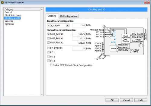
Beyond defining the logic to be implemented on the user-programmable FPGA, LabVIEW simplifies hardware configuration through its project hierarchy and associated configuration pages. For example, the reference clock configuration on these high-speed serial instruments requires a complex algorithm to determine hundreds of register settings to be applied to as many as four separate integrated circuits, in addition to the logic required to apply these registers when the FPGA powers on. LabVIEW FPGA exposes this as a dialog box with a graphical representation of the options, along with design rules and guidance to enforce valid configurations. This approach simplifies the configuration of the any-rate clock synthesizer and routing circuitry to a task that takes minutes rather than hours or days.
Figure 4. LabVIEW FPGA delivers an intuitive, graphical interface for clock configuration that simplifies a complex process.
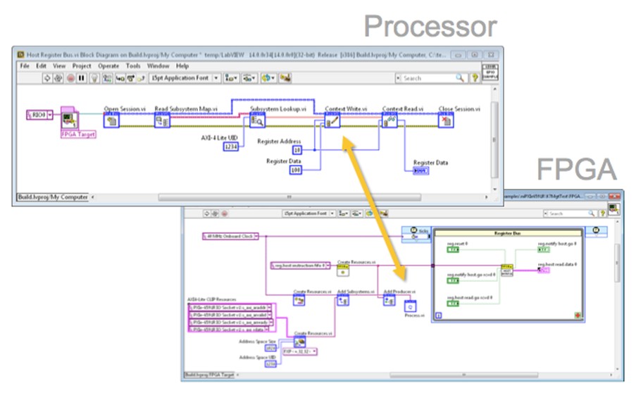
To enable code reuse and simplify common tasks, PXI High-Speed Serial Instruments support certain instrument design libraries, which are host and FPGA code libraries with LabVIEW interfaces designed to work with one another and provide generic capabilities. The Instruction Framework is an instrument design library for dynamic hardware configuration during run time. Though most hardware functionality of these serial instruments (for example, clock configuration) can be statically configured in the LabVIEW project, users can take advantage of the Instruction Framework to control application-specific firmware parameters. For example, the Instruction Framework simplifies the host configuration of register settings exposed through AXI-4 Lite interfaces on the FPGA, commonly found in Xilinx serial protocol IP.
Figure 5. Processor and FPGA code for writing and reading registers through an AXI-4 Lite Interface.
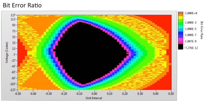
Built on top of the Instruction Framework, the Eye Scan instrument design library provides debug capabilities for the high-speed serial receive channels. The Xilinx GTX transceivers feature two receiver comparators per channel. While one comparator automatically tracks the center of the serial eye based on the recovered clock frequency and phase, the other comparator can independently shift in amplitude and phase. By varying the parameters of the latter comparator and comparing the results with that of the former, the Eye Scan instrument design library can create a statistical eye diagram useful for determining the link margin of the interface, accurate to the bit error rate floor of the Xilinx GTX transceivers. Furthermore, because the Eye Scan instrument design library uses an independent set of hardware resources, it can coexist with other protocol IP and run simultaneously with other application-specific functionality.
Figure 6. The LabVIEW Instrument Design Libraries for PXI High-Speed Serial Instruments includes a reference design for performing statistical eye scan using a loop-back configuration.
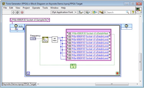
Beyond these instrument design libraries, other NI software-designed instruments provide libraries for a variety of useful functions such as multi-record, as well as DRAM-based acquisition and generation. Though not officially supported or tested on the PXIe-7903, PXIe-7902, PXIe-6594, PXIe-6593, PXIe-6592, and PXIe-6591, depending on the hardware agnosticism of the instrument design library, they may be used with PXI High-Speed Serial Instruments as well.
Figure 7. Engineers can use the DSP instrument design library to synthesize a sinusoid for a transmission to a digital to analog converter over the serial JESD204B protocol.
Protocols
The Xilinx GTX transceivers on the PXI High-Speed Serial Instruments support a broad variety of protocols. NI provides a number of software examples to demonstrate how to integrate common protocols, as well as LabVIEW architectures for several application patterns. Each example comes with a precompiled FPGA bitfile for the supported instrument, along with the associated source code and protocol IP. If this code requires modification for the end application, certain protocols require an IP license from Xilinx to recompile the FPGA. This protocol IP is available for purchase either through Xilinx or resellers such as Avnet or DigiKey.
Xilinx Aurora
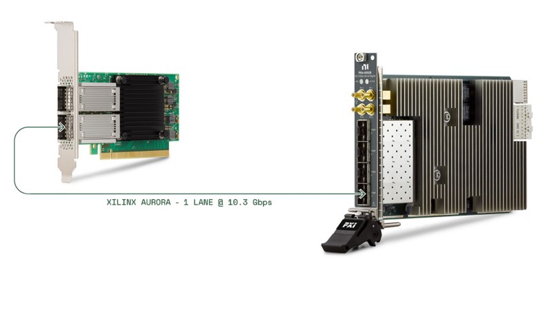
Xilinx Aurora provides a lightweight, low-latency, small-footprint protocol designed for serial point-to-point interfaces. It supports the full rate of the Xilinx GTX serial transceivers, as well as lane bonding for even greater bandwidth. Primarily designed for high-bandwidth data movement, Aurora provides flow control, flexible framing, and options for simplex or full-duplex channels. More information on Xilinx Aurora is at the following links:
http://www.xilinx.com/products/design_resources/conn_central/grouping/aurora.htm
The Instrument Design Libraries for High Speed Serial Instruments driver installs a sample project reference design for Aurora 64b66b, and NI has a web example for Aurora 8b10b.
JESD204B and JESD204C
As analog-to-digital converter (ADC) and digital-to-analog converter (DAC) sample rates and resolutions rise to meet the demands of wireless wideband modulated digital transmissions, data rates to and from these converters have increased. With traditional parallel clock and data interfaces, this calls for more integrated circuit pins with tighter tolerances. JESD204B and JESD204C meet this challenge by transitioning these interfaces to high-speed serial, which is designed to provide high data bandwidth with low latency and to facilitate multiconverter synchronization. JESD204B supports up to 12.5 Gbps and 32 lanes for the latest high-bandwidth, high-speed, and high-channel-count ADCs and DACs. While JESD204C supports rates up to 32 Gbps. JESD204B uses 8B/10B coding while JESD204C supports 8B/10B, 64B/66B, and 64B/80B.
10 Gigabit Ethernet
With a line rate of 10.3125 Gbps, 10 Gigabit Ethernet (10 GbE) provides a practical bandwidth of approximately 1 GB/s. The majority of 10 Gigabit Ethernet interfaces are either optical or SFP+ direct attach (copper), with 8P8C/RJ45-based interfaces. The 10 Gigabit Ethernet example for the PXIe-6592 supports 10GBASE-SR, -LR, and -ER optical interfaces as well as SFP+ direct attach, using the Xilinx 10 Gigabit Ethernet PCS/PMA IP core and the OpenCores.org 10 Gigabit Ethernet media access controller. A lightweight UDP stack implemented in LabVIEW FPGA sits on top of this MAC/PHY solution. More information on 10 Gigabit Ethernet IP cores can be found at the following links:
https://www.xilinx.com/products/intellectual-property/10gbase-r.html
The Instrument Design Libraries for PXI High-Speed Serial Instruments driver installs a sample project reference design for both 1 GbE and 10 GbE.
100 Gigabit Ethernet
100 Gigabit Ethernet (100GbE) can transmit Ethernet frames at a rate of 100 gigabits per second (Gbit/s)—significantly higher speed than 10 Gigabit Ethernet. 100 GbE offers different optical and electrical interfaces and different numbers of optical fiber strands. Some of the key interfaces include 100GBASE-KR2, 100GBASE-CR2, and QSFP28.
LabVIEW FPGA ships with an example for 100 GbE.
CPRI
CPRI defines the optical interface between the radio equipment control (REC) and radio equipment (RE) commonly known as remote radio heads (RRHs). It facilitates radio head configuration and synchronization, as well as streaming digital I/Q (baseband) data. More information on the Xilinx CPRI IP core is at the following link:
https://www.xilinx.com/products/intellectual-property/do-di-cpri.html
Serial RapidIO
Serial RapidIO is a high-performance serial interconnect protocol optimized for energy-efficient embedded systems such as telecommunications infrastructure, military and aerospace embedded computing, high-bandwidth life sciences devices, and industrial control. It features rates up to 6.25 Gbps, four-lane bonding, low latency, flow control, in-order packet delivery, and a relatively small footprint. More information on the Xilinx Serial RapidIO IP core is at the following link:
http://www.xilinx.com/products/intellectual-property/ef-di-srio.html
A reference design of Serial RapidIO for the PXIe-6592 is available on the NI Community. For SRIO interfaces larger than x2, NI recommends the PXIe-6591.
Additional Protocols
The previous examples are not an exhaustive list of all protocols that are compatible with PXI High-Speed Serial Instruments. Local NI sales engineers can answer questions about specific protocols, customizing the above examples, or custom or proprietary protocol integration.
Example Applications
The flexible architecture of the PXI High-Speed Serial instruments gives them the ability to support a variety of use cases, each with different data movement patterns, serial protocols, and software capabilities.
Protocol Functional Test
A common use case for PXI High-Speed Serial Instruments is to perform protocol-specific functional tests on a given DUT. These tests are designed to confirm that the DUT can reliably communicate with the “outside world” through a serial protocol. Such tests might write and read back registers on the DUT, perform data throughput and latency benchmarks, or exercise other protocol-specific attributes or built-in test modes. They might also test how the DUT responds to fault scenarios such as response timeouts, injected errors, or ignored flow control commands. Related tasks include link bit error rate measurements, physical layer stress testing such as maximum and minimum line rates, burn-in testing, and even bus snooping, in which the instrument performs analysis, custom triggering, and data capture on the FPGA.
DUT Control, Stimulus, and Response
Another common use case for PXI High-Speed Serial Instruments is DUT control, stimulus, and response capture. In this scenario, the instrument is not necessarily testing the high-speed serial protocol directly, but rather sending or receiving data from the DUT using a high-speed serial protocol, so that other aspects of the device may be tested. Furthermore, the auxiliary digital I/O can be used to control the DUT using parallel or low-speed serial protocols, such as SPI.
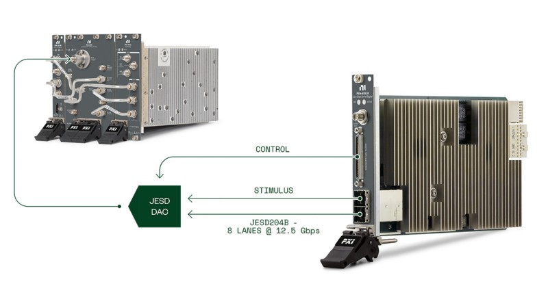
In the following example, a PXIe-6591 stimulates a DAC using the JESD204B protocol in order to test the analog output characteristics of the DAC.
Figure 8. Many modern high-performance DACs and ADCs include communication using the JESD204B high-speed serial protocol.
High-Bandwidth Data Movement
Many high-performance embedded applications can benefit from the PXI platform, and require high-bandwidth, low-latency data movement to and from third-party hardware and NI PXI devices. For these applications, PXI High-Speed Serial Instruments offer benefits such as LabVIEW FPGA hardware processing, P2P data streaming to PXI Express instruments, and high-bandwidth streaming to and from disk, while providing high-bandwidth connectivity to external devices through a standard high-speed serial protocol.
In the following example, an NI oscilloscope samples an analog signal and then sends the raw, digitized data to a PXIe-6592 high-speed serial instrument using P2P data streaming. The instrument then processes the data in real time using an algorithm implemented in LabVIEW FPGA. It finally transmits the processed data to a third-party device using the lightweight Xilinx Aurora protocol, which is designed for FPGA-to-FPGA serial communication.
Figure 9. PXI High-Speed Serial Instruments are an excellent solution for high-bandwidth, low-latency data movement with a third-party device.
Link Debug and Parametric Test
Because high-speed serial interfaces employ very high frequency signals, poor signal integrity can disrupt communication. When such problems arise, debugging tools can provide valuable insight into the state of the link. The Eye Scan instrument design library previously described gives designers the ability to determine link margin on received signals and identify whether communication issues are due to low signal integrity. Although primarily designed for debugging during application development, this functionality may also be employed in device validation or manufacturing test for insight into device-specific performance parameters. However, the PXI High-Speed Serial Instruments feature nominal values for amplitude and timing accuracy, and NI does not provide warranted performance or traceability on these parameters. In-situ calibration or adjustment may be an option for certain applications.
Other parametric tests include the bit error rate for a known pseudo-random bit sequence (PRBS) using industry-standard patterns (PRBS-7, PRBS-15, PRBS-23, and PRBS-31) in lieu of a specific protocol. Transmitter and receiver line rates may be varied to determine the range of supported bit rates for a particular DUT. Finally, transmitter amplitude as well as pre-and post-emphasis may be varied to test receiver sensitivity, including automatic gain control and dynamic equalization.
For the PXIe-6591 and PXIe-6592, you can find additional resources in the NI Community at the following link: NI MGT Debug Tool on the NI Community for more physical layer analysis tools to use with PXI High-Speed Serial Instruments. For the PXIe-6593 and PXIe-6594, reference Using Eye Scan with PXIe-6593 and PXIe-6594 High-Speed Serial Devices.
Skills Required
Although LabVIEW and LabVIEW FPGA dramatically simplify the task of implementing high-speed serial technology, certain expertise is essential to ensure success when programming PXI High-Speed Serial Instruments. Because they are designed in LabVIEW, familiarity with LabVIEW graphical programming is essential. The NI LabVIEW Application Development Training Courses page on ni.com can offer that help. In addition, to customize the non-protocol FPGA logic in LabVIEW FPGA, a detailed understanding of high-throughput LabVIEW FPGA programming is required. The NI LabVIEW High-Performance FPGA Developer’s Guide is a good resource for learning more. For protocols with existing IP or examples, VHDL knowledge and experience is required to define the interface between the protocol IP and the LabVIEW FPGA diagram. Finally, to implement new or custom protocols, advanced digital design expertise is suggested. Certain NI Partners offer these capabilities for those who do not have them in-house. Local NI sales representatives can assist in finding an appropriate partner.
| Use Model | LabVIEW | High Throughput LabVIEW FPGA | VHDL | Extensive Digital Design Expertise |
| Use existing personality | — | — | — | |
| Customize FPGA code, but not protocol | — | — | ||
| Integrate existing protocol | — | |||
| Implement new or custom protocol |
Table 4. Programming high-speed serial instruments requires different levels of skills and tools depending on the level of changes needed in the interface.
Next Steps
- Learn more about Maximizing Data Movement and Signal Processing with the NI PXI High-Speed Serial Module.
- Learn more about the fundamental concepts of high-speed serial communication links.
- See an example reference design for implementing high-speed serial protocols into functional test systems for radio transceivers.
- Get additional protocol reference designs not included in the hardware driver from the Examples and IP for Software-Designed Instruments and NI FlexRIO community.
- Shop PXI High-Speed Serial Instruments.
- Build your PXI System.
