High-Speed Serial Explained
Overview
High-speed serial is an increasingly popular technology that reduces device footprint and increases data communication rates. This paper explores the fundamental concepts of high-speed serial communication links.
Contents
The Need for High-Speed Serial
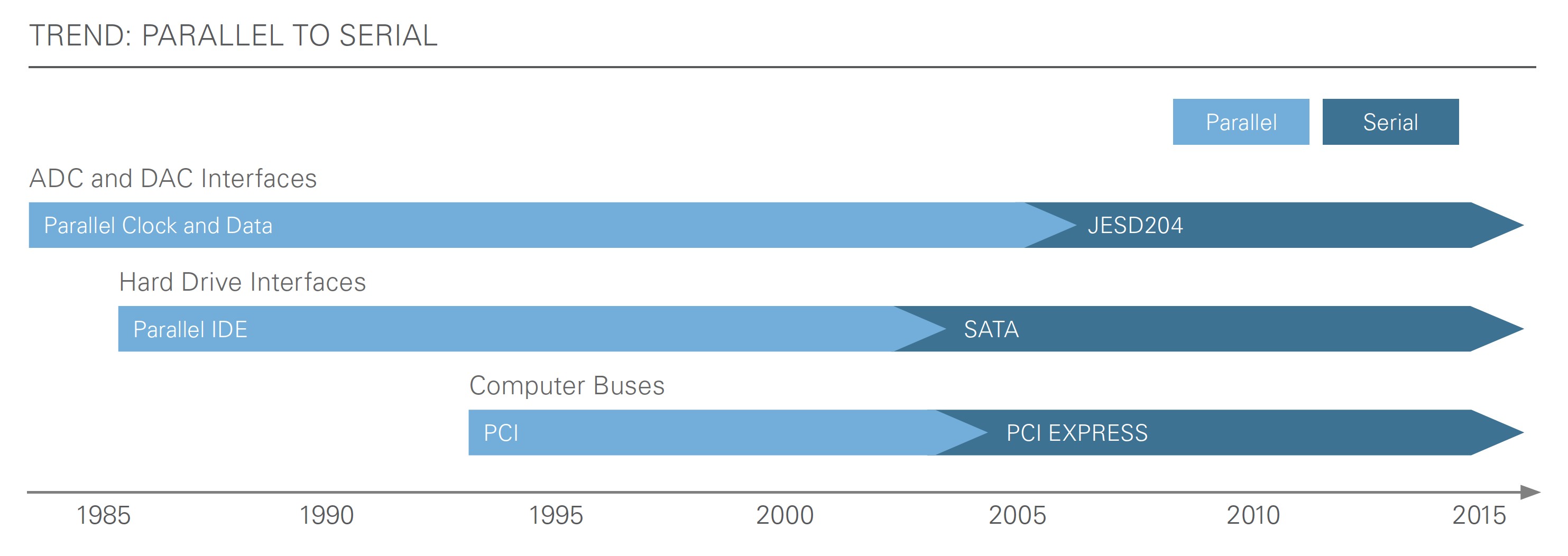
Consumers continually demand better performance in a smaller form factor with reduced power requirements. In the early 2000s, these demands in a world of big data sparked a drastic shift from parallel to high-speed serial digital communication buses. This in turn has led to devices with much smaller footprints, much higher data throughput, and lower power requirements. These features enable many of the technologies that consumers take advantage of today such as SATA, USB, and PCI Express.
Figure 1: In the early 2000s, the market began transitioning from common parallel communication standards to serial standards.
Advantages
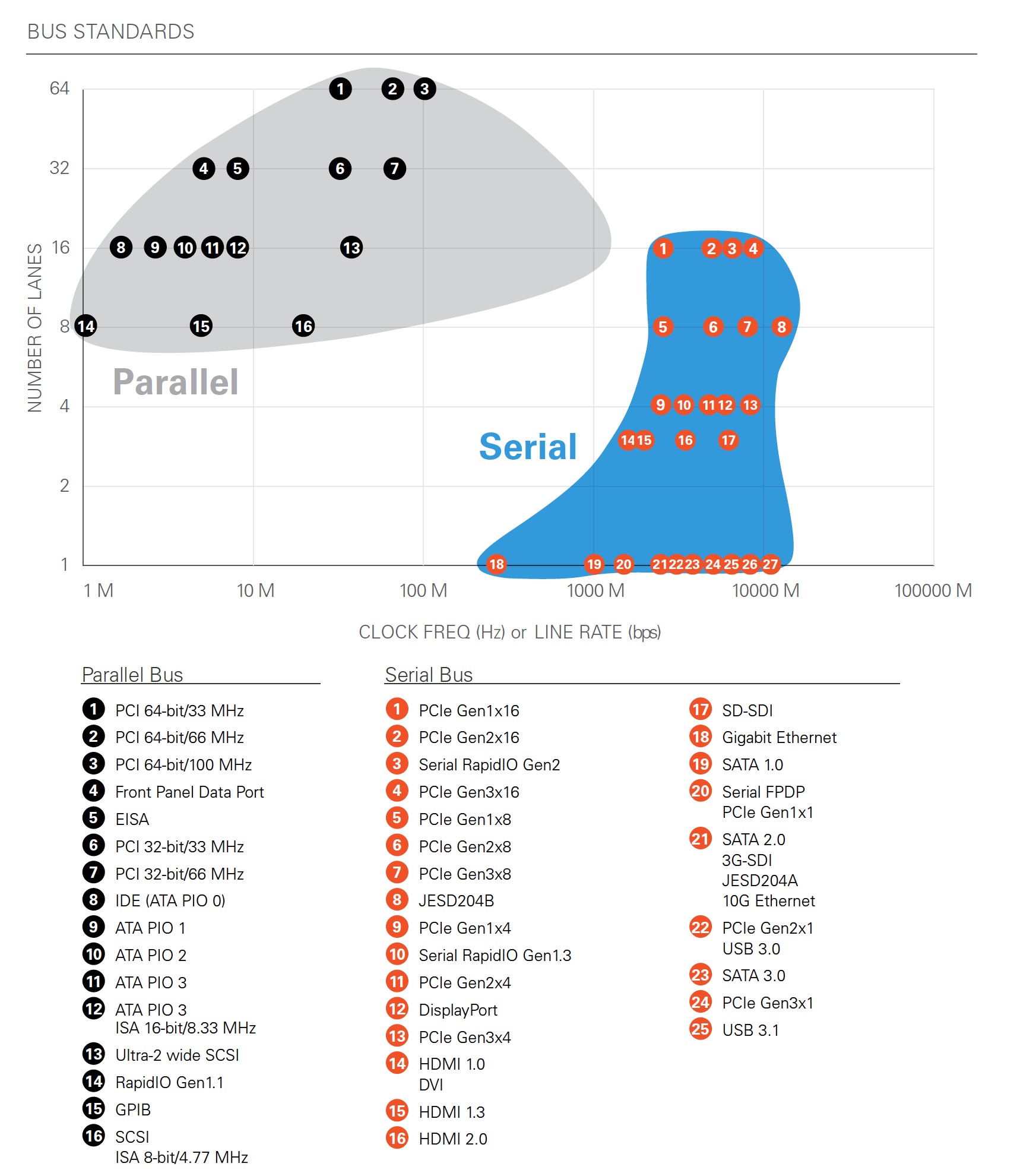
The physical limitation on the clock rates of parallel buses is around 1 GHz to 2 GHz due to the skew introduced by individual clock and data lines that causes bit errors at faster rates. High-speed serial buses send encoded data that contains both data and clocking information in a single differential signal, so engineers can avoid the speed limitations in parallel buses. Today, high-speed serial links with data lanes running at 10 Gbps are common. Additionally, multiple lanes of serial links can be coherently bonded together to form communication links with higher data throughputs.
By serializing the data and sending it at faster speeds, the number of pin counts in integrated circuits (ICs) can be reduced, which helps decrease device size. Furthermore, because the serial lanes can operate at a much faster clock speed, you can achieve better data throughput than that possible with parallel buses.
Figure 2: This chart shows well-known bus standards and their respective numbers of lanes versus line rates. The serial standards are capable of much higher line rates than the parallel standards, leading to higher throughput.
Disadvantages
Though reduced pin count can ease design complexities, the faster speeds required present additional design challenges. With designs reaching RF frequencies, you must make similar analog considerations as you would for RF applications to ensure proper signal integrity. To alleviate these signal integrity issues, you can use high-speed serial links to implement techniques such as encoding, pre-emphasis, and equalization.
Layers of High-Speed Serial Links
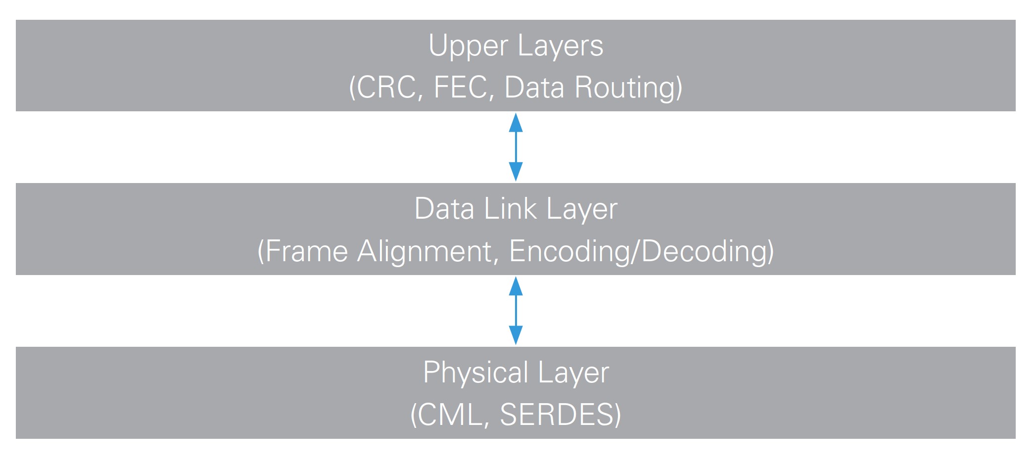
For a serial connection to work, each end must agree to operate within specific parameters. You can abstract these parameters to multiple functional layers.
Figure 3: You can add layers above the physical and data link layer. These layers vary by protocol and application and are typically the most common layers to customize.
Physical Layer
The physical layer ensures electrical compatibility between devices and presents synchronously clocked bits to the data link layer.
Electrical Interface
Different high-speed serial protocols define different requirements for the electrical interface of the transmitter and receiver. This ensures electrical compatibility when connecting the transmitter device to the receiver. The electrical signal for high-speed serial links has difficulty achieving the extremely fast rise and fall times necessary to communicate at speeds above 1 Gbps, minimizing electromagnetic emissions, and improving noise immunity by rejecting common-mode noise. Furthermore, peak-to-peak voltages rarely go above 1 V at these speeds, and electrical standards are typically low-voltage differential signaling (LVDS), emitter-coupled logic (ECL), or current-mode logic (CML).
Clock and Data Recovery
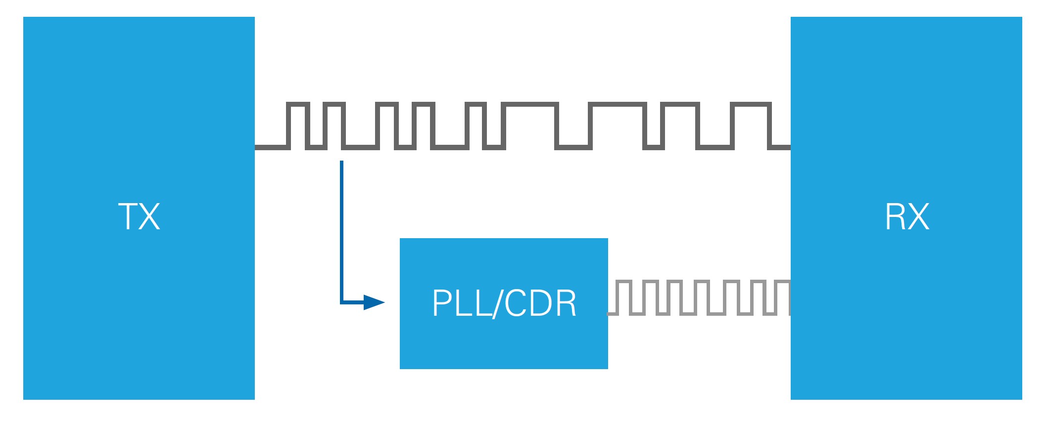
Another important feature of the physical layer for high-speed serial links is clock and data recovery (CDR). CDR is the ability of the receiving device to clock the incoming data stream without the need for an actual clock signal. The data link layer helps achieve this by ensuring frequent bit transitions through encoding. This allows phase-locked loop (PLL) and phase interpolator (PI) circuitry to re-create the transmitting clock and use it to capture the incoming data stream with minimal timing error.
Figure 4: Because encoding at the data link layer ensures frequent transitions between 0 and 1, CDR circuitry can PLL to the incoming bit stream and synchronously sample the encoded data bits.
Signal Integrity Considerations
Transmitting data with bits transitioning at rates of 5 GHz or more creates analog design challenges. Because transmission speeds are now in frequency ranges typical of RF designs, signal integrity issues arise. You need to use high-quality PCBs, connectors, and cables to successfully communicate at these high data rates. Also, PCB designers should understand transmission line theory when designing for high-speed serial links. They need to be able to avoid stubs, impedance mismatch, and trace length mismatch and use proper techniques for minimizing signal distortions.
Equalization
Equalization is the process of counteracting a channel’s electrical behavior to increase its frequency response. This may occur on either the transmitter or receiver side of the communication link to improve link margin, but the term equalization is typically used when referencing the receiver. When the high-speed serial signal travels over the PCB traces, through connectors and cables, and into the receiver, attenuation does not affect all frequency components of the signal equally and causes signal distortion. The equalization settings on multigigabit transceivers (MGTs) can apply gain or attenuation to different frequencies of the signal before it is sampled to improve the signal and link margin. Many MGTs feature auto-equalization to automatically detect and continuously update the equalizers to their ideal settings.
Pre-emphasis
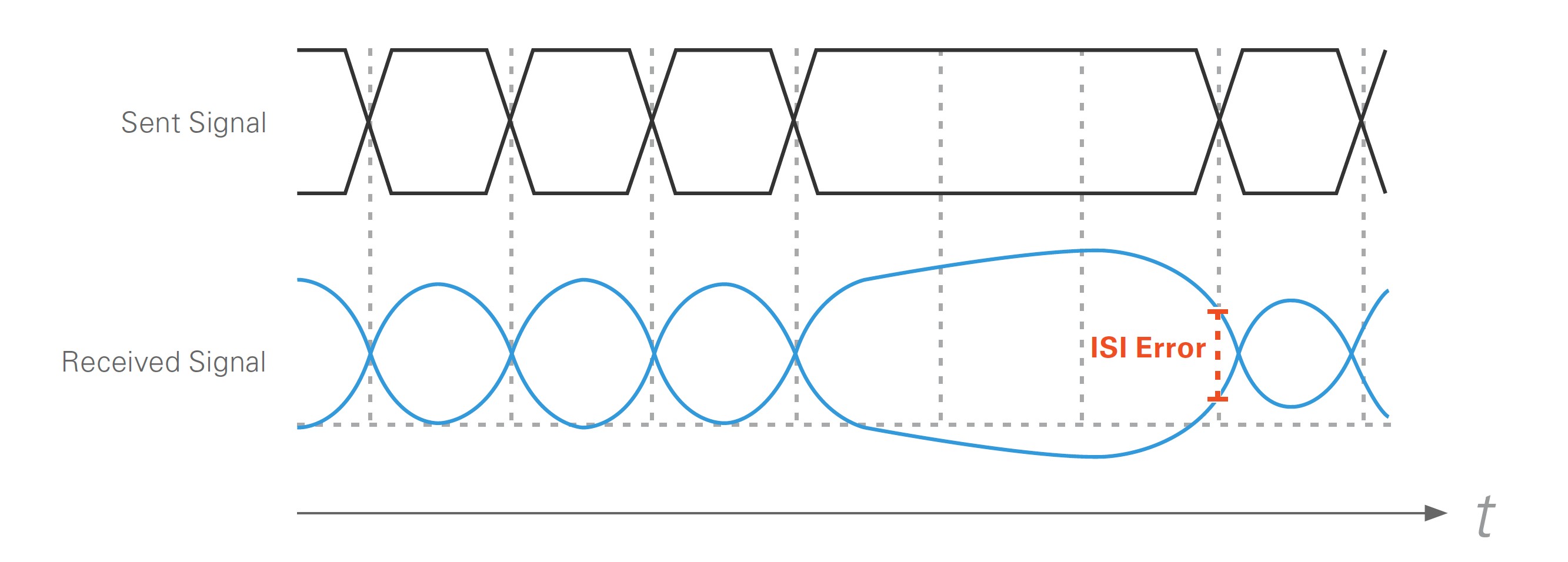
Pre-emphasis typically refers to equalization on the transmitter side of a high-speed serial link. It is primarily used to overcome analog challenges presented by intersymbol interference (ISI). At fast line rates, the data bits start to affect one another when transmitting. For example, if three 1s are transmitted in a row, followed by a single 0, the data line has difficulty driving the 0 low quickly because the line has built up a positive bias.
Figure 5: Signal degradation due to ISI is caused when a lack of bit transitions causes the line to build a bias, making it harder for the first transition to the opposite bit to occur quickly.
You have two ways to overcome ISI. If you know that only the first bit after a transition from low to high or high to low has trouble, you can amplify just the first bit after a transition. This results in the signal shown in Figure 6.
Figure 6: Pre-emphasis is designed to exaggerate the first bit after a transition of a signal. This helps alleviate problems like ISI.
A more common approach to achieving a similar waveform is to attenuate the bits after the first transition instead of amplifying the first bit. Highpass filtering accomplishes this because the transitioning bits (higher frequency) are attenuated less than the nontransitioning bits.
Data Link Layer
The data link layer manipulates data to improve signal integrity, ensure successful communication, and map physical bits to data. Features that enable this are encoding schemes and control characters for alignment, clock correction, and channel bonding.
Encoding Schemes
The goal of encoding is to guarantee frequent bit transitions for successful CDR as well as ensure a DC balance for the data. For successful CDR, the encoding scheme needs to ensure the data signal has enough transitions for the CDR circuitry to remain phase locked to the data stream. If the PLL inside the CDR circuitry cannot stay locked because of a lack of transitions, the receiver cannot guarantee the synchronous clocking of data bits, and bit errors or link failure occurs. You accomplish CDR by ensuring symbols with frequent bit transitions are transmitted, which results in overhead bits being added to the data.
DC balance is also important to maintain a functioning serial link. If you don’t regulate the amount of DC balance, the signals could drift away from their ideal logic high and low levels and bit errors can occur. You ensure DC balance by balancing the statistical amount of 1s and 0s in the symbols that are transmitted. In a DC balanced signal, the number of 0s and 1s transmitted over time are statistically equal over time.
8b/10b Encoding
One common encoding scheme is 8b/10b. For every eight bits of data, two additional bits are added for encoding overhead. These two additional bits provide four times as many bit representations (symbols) as eight bits of data. The 8b/10b encoder narrows down its many symbol options by choosing the predefined symbols with the most transitions and best DC balance to map to specific data words and control symbols. It stores these symbols in look-up tables used to encode and decode the data.
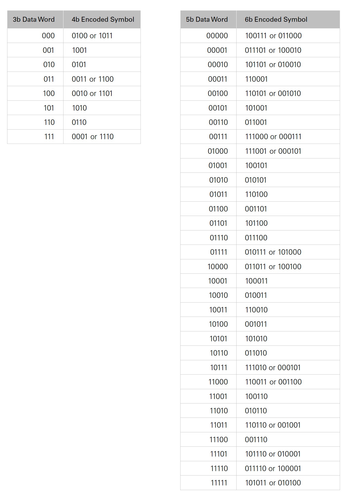
When an 8-bit data word is ready to be encoded, the encoder breaks the data word into five bits and three bits and performs separate 5b/6b and 3b/4b encoding on the data word. It sends the five least significant bits to the 5b/6b table and the three most significant bits to the 3b/4b table.
Table 1: The encoder encodes 8b data words by sending the three most significant bits to a 3b/4b table and the five least significant bits to a 5b/6b table. The encoder then combines them based on running disparity to form a 10b symbol with frequent transitions for CDR circuitry.
In an ideal situation, all symbols have an equal number of 0s and 1s to maintain DC balance. But this is not the case for the symbols in the 5b/6b and 3b/4b tables, so rules were implemented to make decisions based on a concept known as “running disparity.” This is the accumulated difference between the number of 1s and 0s that have been transmitted. Not enough symbols have an equal number of 1s and 0s to represent eight bits, so some data words are represented with two symbols: one symbol with more 0s than 1s and one symbol with more 1s than 0s. For example, the symbol from the 3b/4b table of 1101 also can be represented as 0010. When choosing which version of the symbol to use, the encoder always tries to balance the running disparity. The disparity of a full 8b/10b symbol is always 0, +2, or -2. Table 2 shows the encoder’s process for deciding which symbol it should use.
Table 2: The rules for running disparity determine which version of the code word is used to ensure DC balance.
For example, consider encoding the data word 10010001. The three most significant bits (100) are sent to the 3b/4b table, and the five least significant bits (10001) are sent to the 5b/6b table. If this is the first word being sent on the line, the encoder assumes a -1 disparity; therefore, this example assumes the running disparity is -1. The 5b/6b portion has no choice to make, while the 3b/4b portion decides whether the disparity is +2 or -2. Because the running disparity is -1, the 3b/4b code with disparity +2 (1101) is chosen. When the 3b/4b and 5b/6b codes are combined, the total encoded symbol is 1101100011. After this symbol is transmitted, the running disparity is now +1 = -1 + 2.
64b/66b Encoding
Using a different approach than 8b/10b encoding, 64b/66b encoding can accomplish similar tasks. Instead of code tables, it uses scrambling. Scrambling requires a hardware circuit that offers a high probability of multiple, somewhat evenly spaced 0s and 1s. Scrambling allows the encoded data to appear random with frequent transitions, but it can still be unscrambled on the receiver side.
Figure 7: A scrambling circuit makes the output data appear random and DC balanced, but the data can still be descrambled on the receiver. Scrambling is an alternative method to encoding data with a look-up table.
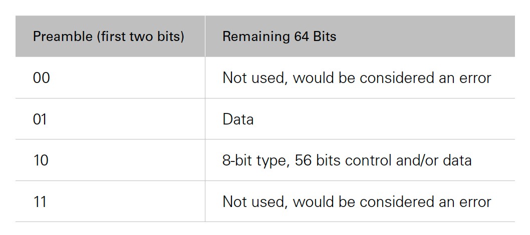
The first two of the 66 bits are considered the preamble, and they provide information about the remaining 64 bits. The main advantage of 64b/66b compared with 8b/10b is the reduced overhead. The 64b/66b features a little over 3 percent overhead, while the 8b/10b has 20 percent overhead. One drawback of 64b/66b encoding is that it has no bound on the DC balance like 8b/10b encoding does. Though the scrambling circuits have proven to be very good at appearing random and having a statistically insignificant DC imbalance, 64b/66b encoding is not bounded like 8b/10b.
Table 3: The first two bits of a 64b/66b symbol are considered a preamble. The preamble provides information to the decoder about the 64 bits that follow the preamble. The Table 3 preamble meanings apply to 10 Gigabit Ethernet.
64b/67b
Certain electronics are too sensitive to DC offset over time. This may be the case for the 64b/66b encoding scheme. It might not be attractive to designers because the DC offset is not bounded. In these situations, engineers are stuck with the higher overhead (20 percent) of the 8b/10b scheme. The 64b/67b scheme adds one additional bit of overhead, which allows it to limit the running disparity to ±96.
The transmitter monitors the running disparity and calculates the new scrambled code words disparity. If the new code word is going to lower the disparity number, it transmits that symbol. If the new code word is going to increase the disparity number, the encoder flips the 64 scrambled bits (no need to flip the preamble with the disparity of zero). The additional bit is referred to as the inversion bit, and it informs the decoder whether the decoder needs to invert the data or not. This allows chip electronics that are sensitive to DC offset to benefit from a low-overhead encoding scheme that also exhibits a bounded DC offset.
128b/130b
PCI Express 1.0 and 2.0 both use 8b/10b, while PCI Express 3.0 and 4.0 made the jump to 128b/130b to have higher data throughput with an achievable line rate. Think of the 128b/130b scheme as 64b/66b with a doubled payload and still only two preamble bits. Table 4 shows the specifications for PCI Express.
Table 4: This table shows the specifications for the four generations of PCI Express. PCI Express 3.0 and 4.0 transitioned to 128b/130b to increase their data throughput while keeping their line rates at a more manageable speed.
Control Symbols (K-Characters)
Control symbols, also known as k-characters when referring to 8b/10b encoding, are an important function of high-speed serial links. They are symbols that can be differentiated from data, so the receiver can use them for different control responsibilities, such as byte boundary alignment before decoding, clock correction techniques, and channel bonding for data coherency across multiple lanes.
Alignment and Comma Detection
For decoding to work correctly, the receiver needs to know the correct word boundaries of the encoded data. The receiver scans the incoming data for the control character, which is also referred to as a comma when used for alignment in the 8b/10b scheme. The control character defines the boundary of the encoded data. Once the receiver has identified the alignment character, it has a concept of word boundaries for the encoded data, so the encoded data can be sent to the decoding logic.
Clock Correction Characters
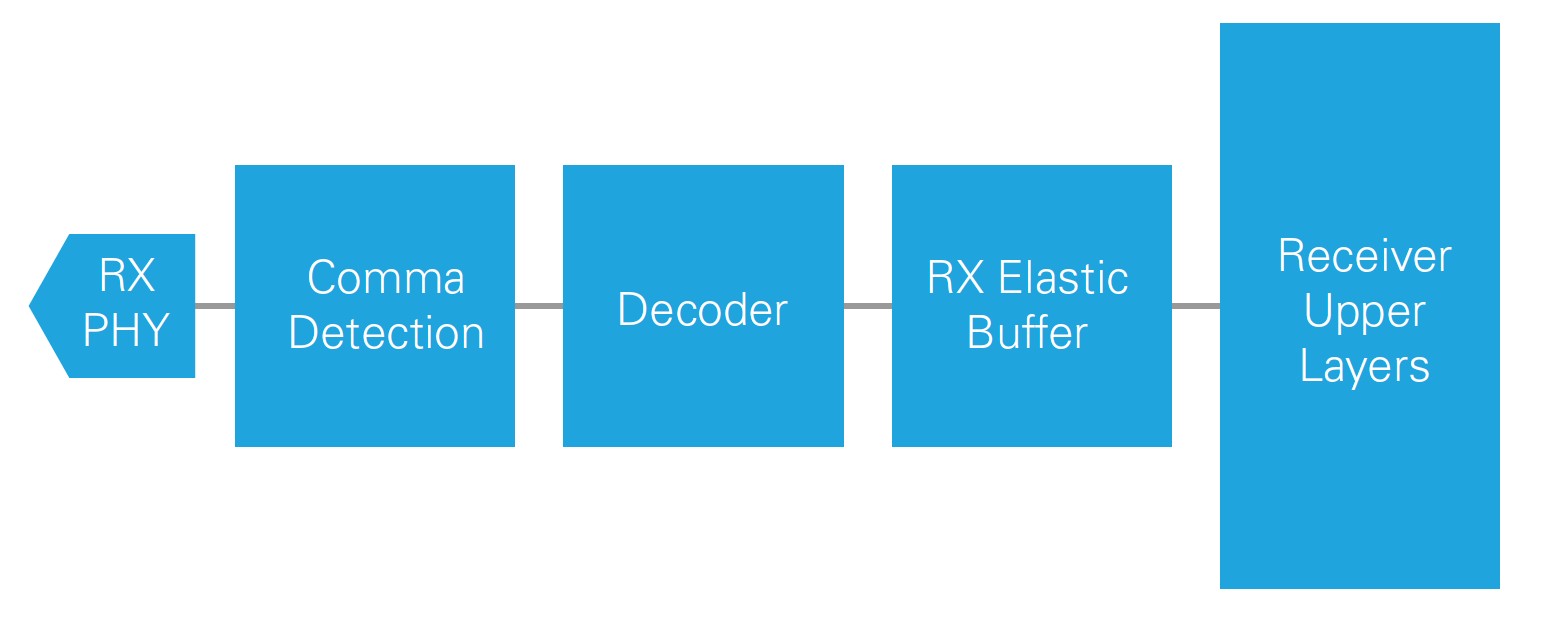
Clock correction is required whenever the transmit clock is not locked to the same source as the receive clock. Even if these clocks are on the same nominal frequency, they slowly drift apart because of small amounts of clock frequency inaccuracies. Having a first-in-first-out memory buffer (FIFO), sometimes referred to as an elastic buffer, allows the receiver to account for minor clocking differences between the transmitter and receiver and implement clock correction.
Figure 8: The RX elastic buffer between the decoder and receiver upper layers is required to implement clock correction. It buffers data to prevent errors due to unlocked clocks drifting from each other and enables communications between two devices without their sharing a reference clock.
Clock correction logic ensures that the elastic buffer never underflows or overflows. If the transmit clock is running slightly faster than the receive clock is reading from the elastic buffer, overflow can occur if you don’t have clock correction techniques. If the transmit clock is running slightly slower than the reading logic on the receiver, than underflow can occur if you don’t have clock correction.
A control character is chosen as a clock correction character. The transmitter sends this clock correction character periodically interleaved with real data, and the frequency of that clock correction character depends on the clock correction needs of the application and hardware design. If the clock correction logic on the receiver detects the elastic buffer on the receiver is going to underflow, the receiver correction logic can insert additional clock correction characters to ensure buffer underflow doesn’t occur. If the clock correction logic detects the elastic buffer is getting too full and is ready to overflow, the logic can throw away the clock correction sequences in the buffer to create additional room for data.
Channel Bonding
If the line rate and encoding scheme cannot deliver the data throughput you need on a single serial lane, you can use multiple lanes. For example, HDMI standards use three serial data lanes to achieve their overall data bandwidth. When sending data across multiple lanes, propagation delays cause the data to arrive at different times to each receiving lane at the receiver. Depending on the application, you may need to align the data across all lanes at the receiver, a process known as channel bonding. The elastic buffer in each receiving lane at the receiver used for clock correction is also used for channel bonding.
To achieve channel bonding, you must choose a special control character and reserve it for channel bonding. The serial link has one master lane, and the rest are considered slaves. The master and all slaves send the channel-bonding character at the same time from the transmitters. When the master receiver sees the channel-bonding sequence in a certain location of the elastic buffer, the master receiver instructs all slaves to find their bonding sequences and adjusts the read pointers of all elastic buffers to the offset of the channelbonding sequence location. Because each data lane has its own offset for its own elastic buffer, the receiver can read from different locations of each elastic buffer, which results in reading aligned data.
Figure 9: Channel bonding changes the read pointers of the elastic buffer on each receive lane to allow the receiver to read synchronous data across multiple data lanes.
Idle Characters
Another important use case for control characters is the idle character. For the clock and data recovery to stay phase locked, the transmitter must continuously send bits. When it has no data to send, it must send an idle character. This is another control character determined by the protocol, and the receiver knows that character is not true data.
Additional Upper Layers
Additional upper layers sit above the data link layer to help you tailor the communication to your specific needs. Some protocols have specific standards for upper-layer features, and other protocols leave that up to you. Common communication customizations include error checking/correction, header information for packet-based communication, or even link status information.
The layers above the data link layer and physical layer are the layers most commonly customized for application-specific needs. Some examples of common upper-layer customizations are error detection and correction through cyclic redundancy checking (CRC) and forward error correction (FEC). As a trade-off for data transfer efficiency, you can use schemes to detect or correct errors. CRC implements rules to detect bit errors in the transmission but cannot correct the errors. You can customize the application to re-request data. FEC, on the contrary, contains additional error correction information in the transmitted data that can allow the receiver to recover from a limited amount of bit errors. This is useful for noisy channels or communication rates so high that bit errors due to signal integrity are more common. Including FEC is a design decision that sacrifices data rate efficiency for relaxed signal integrity requirements.
Conclusions
You must overcome many challenges at multiple layers of the high-speed serial link to successfully communicate. Having an understanding of the different concepts at each level helps you implement and test different layers. For any one layer to work, the layers below it need to be functioning correctly. By using one of the many defined specifications for physical and data link layers, you don’t have to determine the low level details on your own. Another benefit of using a standard physical and data link layer is the Internet protocol (IP) that implements all these low-level details for you. A great example of this is the Xilinx Aurora Protocol, a free IP that implements a lightweight, data link layer protocol for point-to-point serial communication. This helps you abstract the small details like clock correction, channel bonding, idle character, encoding/decoding, and more, so you can focus on your upper, application-specific layers.
With the benefits of reduced size and power, paired with increased performance, high-speed serial links are quickly growing in popularity. The communications industry is continually improving high-speed serial technologies to achieve faster line rates and enable the world of big data.
