Highly Parallel Wafer Level Reliability Systems With PXI SMUs
Overview
Reliability testing has long served as a method of ensuring that semiconductor devices maintain their desired performance over a given lifetime. As IC manufacturers continue to introduce new and innovative processes with decreasing device geometries, they need to ensure the additional complexity from these changes does not affect the long-term reliability of their ICs. Additionally, major technology trends in autonomous driving, cloud-based data storage, and life sciences are forcing IC suppliers to provide higher assurances of product reliability to their customers who work on mission-critical applications.
These two trends are driving semiconductor manufacturers to vastly increase the amount of reliability data they collect and analyze while decreasing the cost of test. When faced with this problem of more data at a lower cost, many reliability engineers find they cannot solve it using traditional reliability solutions, so they are turning toward modular, flexible solutions that can scale to fit their needs.
Contents
- Reliability Testing
- Wafer-Level Reliability
- Traditional Approach to Building WLR Systems
- A New Approach for Building WLR Systems
- PXI: A Competitive Advantage
- Learn More
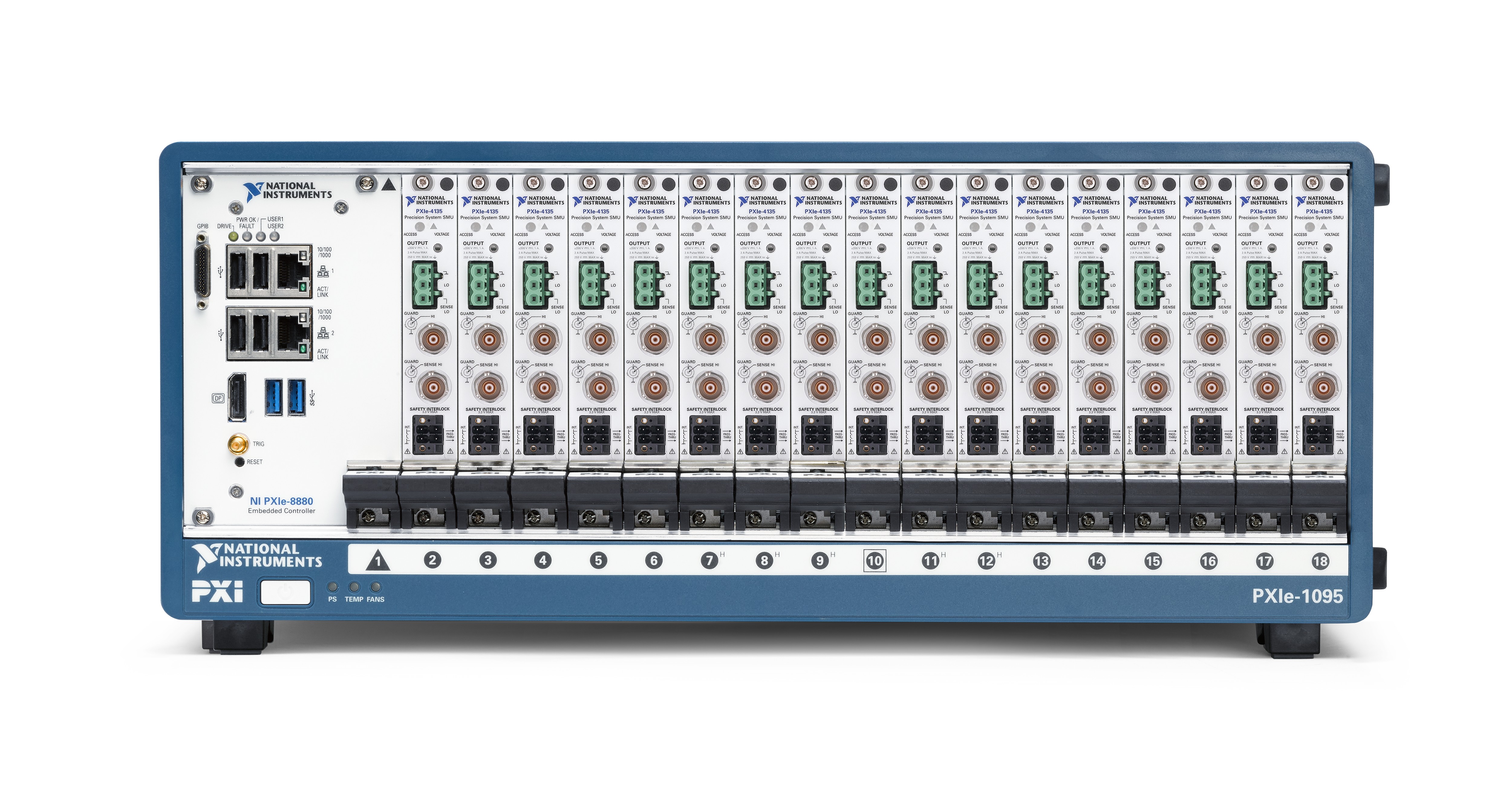
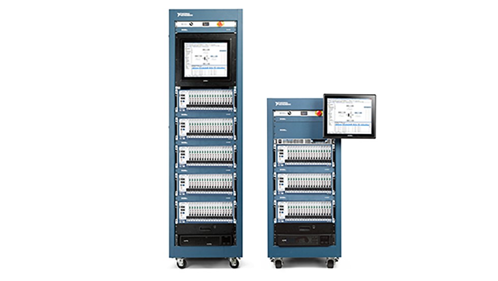
Figure 1. The modular PXI platform provides scalable, high-density solutions for test applications.
Reliability Testing
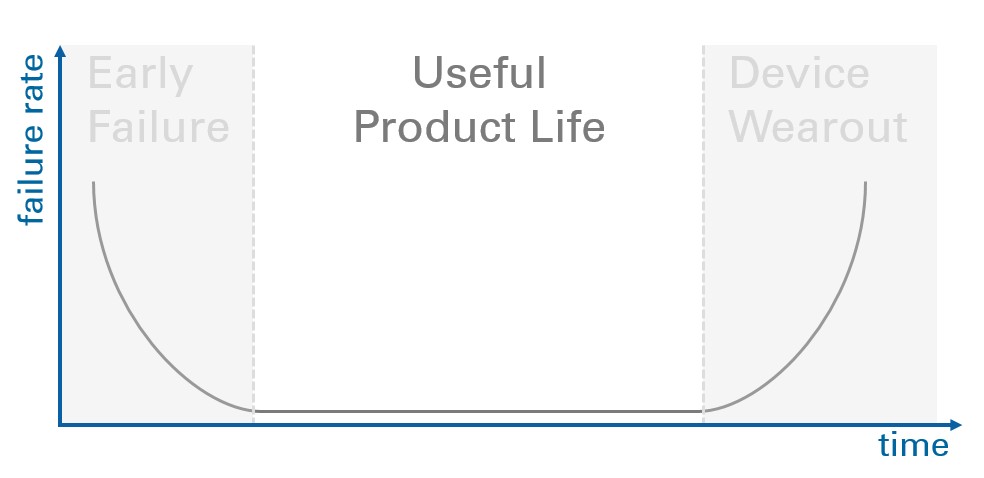
Device reliability is typically modeled as failure rate over time, with the highest failure rates occurring immediately after manufacturing and again after the product has exceeded its useful lifetime.
Figure 2. A Typical Model of Device Reliability
The left side of the graph shows early failures often caused by defects in the manufacturing process. These types of failures can be screened during production to minimize the number of defective parts sent to customers. However, the functional tests performed during production cannot identify defects that cause the device to wear out prematurely and cannot offer insight into the product’s usable lifetime. But reliability testing identifies these types of failure mechanisms and estimates the product’s usable lifetime.
The purpose of reliability testing is to identify these types of failure mechanisms and estimates the product’s usable lifetime.
Reliability testing involves stressing a device at the extreme ends of the device’s specifications—usually voltage and temperature—to accelerate device wearout and model the usable lifetime against known failure mechanisms. These tests can be performed on a wafer or packaged part. Wafer-level reliability (WLR) provides more data earlier in the manufacturing process without the cost and potential damage associated with cutting and packaging the IC.
Wafer-Level Reliability
WLR is a type of parametric testing that extracts information about the device’s usable lifetime and long-term reliability. These tests are typically not performed on the actual IC being developed but rather a set of test structures or purpose-built dies that are built into the wafer specifically for gathering parametric data. These test structures consist of fundamental wafer elements (e.g. transistors, capacitors, and resistors) or basic circuits (e.g. ring oscillator), which provide insight into the fabrication process. Most WLR tests involve applying a stress, such as voltage or temperature, and measuring the response of the device to monitor for any signs of degradation. Common failure mechanisms used include bias or negative bias temperature instability (BTI or NBTI), hot-carrier induced degradation (HCI), time-dependent dielectric breakdown (TDDB), and electromigration (EM).
Traditional Approach to Building WLR Systems
Traditional WLR systems vary in both measurement capability and architecture. Specialized WLR systems may involve high-frequency AC or pulsed stimulus; however, most CMOS devices are tested with DC instruments such as source measure units (SMUs), which provide the necessary stress and measurement capability for collecting parametric data. The two main approaches for building WLR systems involve either building a rack-and-stack system from traditional box instruments or buying a purpose-built turnkey system.
Rack-and-Stack Systems
SMUs are traditionally expensive, high-precision DC instruments that tend to limit the number of channels you can place in a standard test rack. Because of these constraints, SMUs are often combined with a low-leakage switching matrix to route signals from the SMU to dozens of test points while minimizing the noise, leakage current, and thermal EMF associated with relays. This approach works reasonably well when serially testing a small number of test structures generates statistically significant reliability data. Additionally, switching is a practical extension of a box instrument that historically has cost $5,000 to $10,000 per channel and would otherwise be limited to 20 or 40 channels in a full 19 in. test rack. However, given the performance expectations for the relays, the switching subsystem is often a large and expensive piece of the WLR system.
Turnkey Systems
The alternative approach is to purchase a purpose-built turnkey system that is prepackaged with all components such as the oven, test rack, instrumentation, and software. Aligning your test requirements with the functionality of the equipment saves development and integration time but requires a large capital budget. These systems are often built with a fixed number of channels, hardware specifications, and software, and are serviced by the vendor. System vendors may sell separate systems for wafer and packaged reliability systems, or they may sell the same system for both applications regardless of the differences in test requirements.
Challenges of Traditional WLR Systems
The traditional WLR approaches of either buying purpose-built systems or building rack-and-stack systems from box instrumentation served their purpose for decades. However, many engineers are finding these architectures do not scale well to meet their evolving data and cost requirements.
Turnkey systems do not provide the flexibility needed to modify the test software or hardware as device requirements change, or the modifications are prohibitively expensive.
Rack-and-stack systems are limited by the low-channel density of traditional box SMUs. As reliability stresses often require fixed stimulus times, the best way to increase data velocity, or the amount of data that can be gathered in the same (or less) time, is by increasing parallelism. The limited channel density of traditional box SMUs creates challenges for building high-channel-count systems with a small footprint and often forces engineers to use a switched topology to multiplex the SMU to multiple pins. However, this switched topology quickly becomes a bottleneck because the pins are tested serially instead of in parallel, failing to achieve the desired goal of increased data velocity.
Because of these challenges, many companies are starting to build parallel test systems using modular instrumentation.
A New Approach for Building WLR Systems
The market for test instrumentation has changed dramatically over the past decade with the rise of modular platforms such as PXI. Modular platforms have grown increasingly desirable for building automated test systems because of their extensive I/O capability, compact form factor, and flexible software.
Figure 3. Industry analysts predict PXI will continue to be the dominant modular platform.
Using a modular approach, you can dramatically reduce the footprint of WLR systems without sacrificing measurement quality. The open software architecture allows you to define the functionality of your system, modify tests, and add hardware as your requirements change. This includes integrating the latest multicore processors, maximizing system uptime through health and monitoring tools, and adding I/O.
Figure 4. Accelerate Time to Market with Highly Parallel Wafer Level Reliability Testing
High Density Source Measure Units
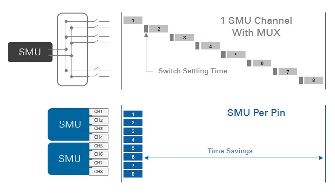
By using PXI SMUs as the foundation for WLR systems, you can add hundreds of SMU channels to your system while maintaining a reasonable footprint and cost per channel. NI SMUs are designed for building automated test systems, and you can use the modular architecture to optimize the number of channels and device specifications of your overall system. With the high-channel density, you can avoid placing switches between the SMU and the wafer. Instead, you can connect each test pad directly to a high-precision device. This “SMU per pin” architecture prevents the negative impact that switches have on signal integrity, test time, and test routine flexibility to help you implement advanced stress-measure algorithms.
Figure 5. A highly parallel, SMU-per-pin architecture can significantly reduce total WLR cycle time compared with a traditional multiplexed architecture.
Though the SMU-per-pin architecture is not completely new to WLR systems, NI SMUs provide a significantly higher number of channels than existing solutions. A WLR system based on PXI SMUs offers the following:
- High density—You can fit up to 68 SMU channels in a single 4U, 19 in. PXI chassis and mount several chassis in a single automated test rack to achieve hundreds of independent SMU channels per system.
- High-precision measurements—With measurement sensitivity ranging from 10 fA to 10 pA, you do not sacrifice the measurement quality of the system.
- High-speed sequencing engine—You can stream large, hardware-timed sequences to SMUs in your system and synchronize all channels. This provides very fast execution rates and deterministic sourcing and sampling.
- Built-in digitizer—With sample rates greater than 600 kS/s, you can capture transient device recovery behavior without an external oscilloscope.
See why users are switching to NI SMUs
High Uptime and Serviceability
Ensuring system uptime is critical for both inline and offline reliability systems. If an inline system fails, wafer production can come to a halt. Offline reliability tests, which are often executed over the course of months or years, offer critical data on the product’s expected lifetime. Because of these requirements, reliability testers need to stay online and continuously collect data throughout the experiment because a failed tester could lead to a failed experiment.
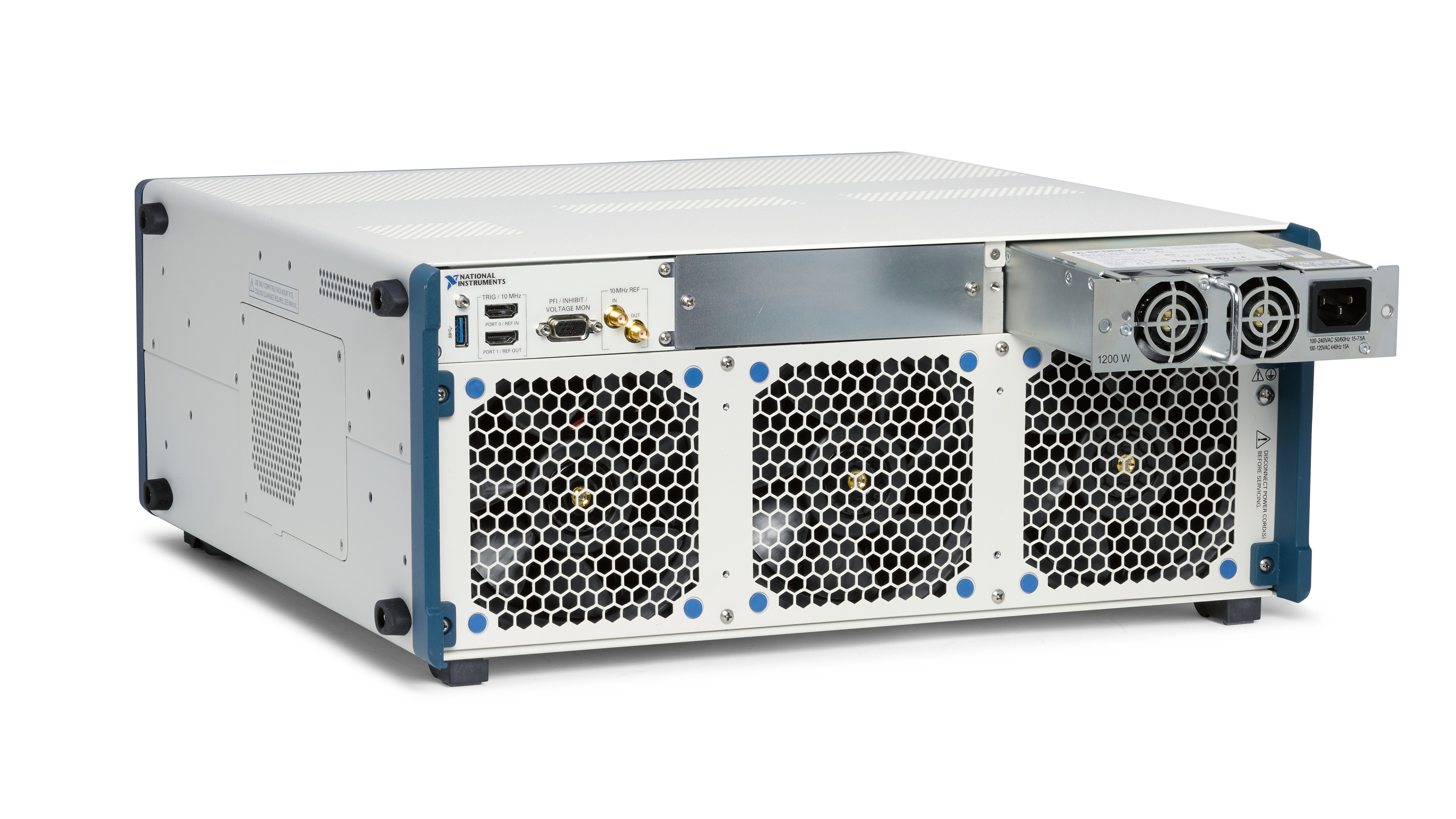
Figure 6. High-Uptime PXI Chassis With Redundant Fans and Power Supplies
The PXI platform provides numerous benefits for developing high-uptime, critical applications. For example, you can build your system using a chassis that has redundant, hot-swappable fans and power supplies. If a component malfunctions, the system continues to run and allows you to replace the component without powering down the system and aborting your experiment. Additionally, you can remotely monitor the health of your system for fan speed, temperature, power consumption, and other key parameters that may indicate an imminent failure.
See how PXI can improve your system reliability, availability, serviceability, and manageability
Access to the Latest Commercial Processors
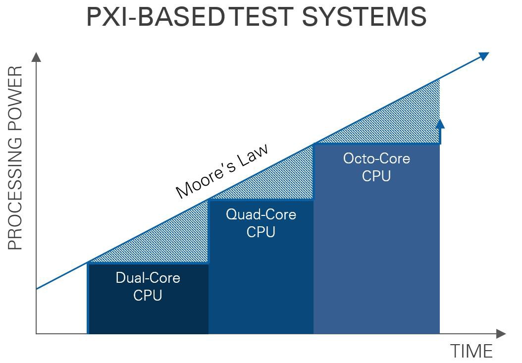
Parallel test systems cannot be bottlenecked by a lack of processing capability or communication latency. One advantage of building parallel WLR systems with PXI is the ability to use controllers with the latest multicore Intel processors. Additionally, the chassis backplane allows for low-latency communication between the processor and modules as well as module-to-module communication with digital triggers. For parallel WLR systems, this means you can offload the detailed sequence execution to each SMU and reserve the controller for data collection and analysis.
Figure 7. PXI-based test systems provide access to the latest commercial processors
PXI: A Competitive Advantage
Traditional reliability systems have served their purpose for decades; however, the ability of these systems to provide and analyze massive amounts of reliability data is decreasing. To address these needs, many companies are turning to modular platforms, such as PXI, for highly parallel WLR systems with high uptime and the latest commercial processors. Using the software-defined architecture of these systems, companies can maintain control of their intellectual property and scale their systems as requirements change. This approach satisfies their need for more reliability data at a lower cost, and positions them well to address ever changing test requirements in the future.
