PXIe-5820 Specifications
- Updated2025-04-22
- 21 minute(s) read
PXIe-5820 Specifications
Definitions
Warranted specifications describe the performance of a model under stated operating conditions and are covered by the model warranty.
Characteristics describe values that are relevant to the use of the model under stated operating conditions but are not covered by the model warranty.
- Typical specifications describe the performance met by a majority of models.
- Typical-95 specifications describe the performance met by 95% (≈2σ) of models with a 95% confidence.
- Nominal specifications describe an attribute that is based on design, conformance testing, or supplemental testing.
Specifications are Warranted unless otherwise noted.
Conditions
Warranted specifications are valid under the following conditions unless otherwise noted.
- Over ambient temperature range of 0 °C to 45 °C.
- 30 minutes warm-up time.
- Calibration cycle is maintained.
- Chassis fan speed is set to High. In addition, NI recommends using slot blockers and EMC filler panels in empty module slots to minimize temperature drift.
- Calibration IP is used properly during the creation of custom FPGA bitfiles.
Typical specifications do not include measurement uncertainty and are measured immediately after a device self-calibration is performed.
Unless otherwise noted, specifications assume the PXIe-5820 is configured in the following default mode of operation:
- I/Q IN voltage range: 2.0 Vpk-pk differential
- I/Q IN common-mode voltage: 0 V
- I/Q OUT voltage range: 1.0 Vpk-pk differential
- I/Q OUT common-mode voltage: 0 V
- I/Q OUT load impedance: 100 Ω differential
PXIe-5820
Pinout
Use the pinout to connect to terminals on the PXIe-5820 .
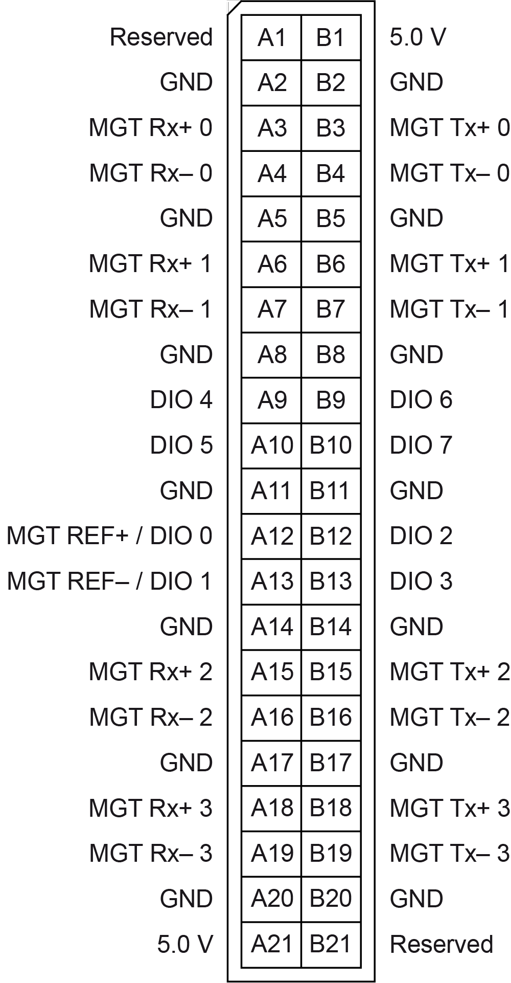
| Signal | Type | Direction |
|---|---|---|
| MGT Tx± <3..0> | Xilinx Virtex-7 GTH | Output |
| MGT Rx± <3..0> | Xilinx Virtex-7 GTH | Input |
| MGT REF± | Differential | Input |
| DIO <1..0> | Single-ended | Bidirectional |
| DIO <7..2> | Single-ended | Bidirectional |
| 5.0 V | DC | Output |
| GND | Ground | — |
Differential Operation
The I/Q inputs and outputs of the PXIe-5820 support differential operation. This section explains some of the fundamental analog signal processing that occurs in the first stages of the I/Q receiver.
A differential signal system has a positive component (VINPUT(CH+)) and a negative component (VINPUT(CH-)). The differential signal can have a common-mode offset (VIN_COM) shared by both VINPUT(CH+) and VINPUT(CH-). The differential input signal is superimposed on the common-mode offset. The input circuitry rejects the input common-mode offset signal.
In a differential system, any noise present on both VINPUT(CH+) and VINPUT(CH-) gets rejected. Differential systems also double the dynamic range compared to a single-ended system with the same voltage swing. The following figure illustrates the key concepts of differential offset and common-mode offset associated with a differential system.

where
- VIN_PP+ represents the peak-to-peak amplitude of the positive AC input signal
- VIN_PP- represents the peak-to-peak amplitude of the negative AC input signal
- VDO represents the differential offset voltage
- VIN_COM represents the common-mode offset voltage
- VOUT_PP represents the peak-to-peak amplitude of the output signal
In the previous figure, the input common-mode voltage is not present after the first stage of the receiver system. The signal remaining at the output of the receiver circuitry is the signal of interest.
In an I/Q analyzer, a differential offset can occur because of LO leakage or harmonics. In the case of I/Q generation, a differential offset can cause spurs and magnitude error.
In a phase-balanced differential system, the peak-to-peak amplitude of the positive AC input signal (VIN_PP+) is equal to the peak-to-peak amplitude of the negative AC input signal (VIN_PP-). The AC peak-to-peak amplitude of the output signal is the sum of VIN_PP+ and VIN_PP-. A more general definition for the output voltage regardless of phase is the difference between VIN_PP+ and VIN_PP- described by the following equation:
VOUT = (VINPUT(CH+)) - (VINPUT(CH-))
The common-mode offset, which represents the rejected component common to both signals, is described by the following equation:
VIN_COM = [(VINPUT(CH+)) + (VINPUT(CH-))]/2
Frequency
Internal Frequency Reference
Initial adjustment accuracy | ±200 × 10-9 |
Temperature stability | ±1 × 10⁻⁶, maximum |
Aging | ±1 × 10⁻⁶ per year, maximum |
Accuracy | Initial adjustment accuracy ± Aging ± Temperature stability |
I/Q Input
I/Q Input Common-Mode Accuracy
| Common-Mode (V) | Accuracy (mV) at 23 °C | |
|---|---|---|
| -0.25 to 1.50 | ±2.5 | |
|
Conditions: Measured with a DMM. Common-mode offset is not adjusted during self-calibration. Valid for vertical ranges between 0.1 Vpp and 2.0 Vpp, differential. Measured with both input terminals terminated to ground through a high impedance >1 MΩ. |
||
I/Q Input DC Offset
| Reference Location | DC Offset at 23 °C ± 5 °C |
|---|---|
| At ADC | <-57 dBFS |
| At connector | <10 mV |
| Conditions: Terminated with 100 Ω differential impedance. | |
I/Q Input Absolute AC Gain Accuracy
| Input Vertical Range (Vpp, Differential) | 23 °C ± 5 °C | 0 °C to 45 °C | |
|---|---|---|---|
| 0.5 to 4.0 | ±0.57 | ±0.71 | |
| ±0.15, typical | ±0.28, typical | ||
| 1.0 to 4.0 | ±0.44 | ±0.57 | |
|
Conditions: Valid for all common-mode voltages. Measured with 10 MHz CW tone from a 100 Ω differential source. This specification is valid only when the module is operating within the specified ambient temperature range and within ±5 °C from the last self-calibration temperature, as indicated by the niRFSA Device Temperature property or NIRFSA_ATTR_DEVICE_TEMPERATURE attribute. |
|||
I/Q Input Frequency Response
| Frequency | Input Vertical Range (Vpp, Differential) | 23 °C ± 5 °C | 0 °C to 45 °C |
|---|---|---|---|
| 100 kHz to 100 MHz | 0.5 to 4.0 | ±0.31, typical | ±0.36, typical |
| ±0.82 | ±0.92 | ||
| 1.0 to 4.0 | ±0.67 | ±0.77 | |
| 100 kHz to 250 MHz | 0.5 to 4.0 | ±0.31, typical | ±0.36, typical |
| ±0.82 | ±0.97 | ||
| 1.0 to 4.0 | ±0.67 | ±0.83 | |
| 100 kHz to 500 MHz | 0.5 to 4.0 | ±0.31, typical | ±0.62, typical |
| ±0.82 | ±1.22 | ||
| 1.0 to 4.0 | ±0.68 | ±1.10 | |
| 10 MHz to 250 MHz | 0.5 to 4.0 | ±0.10, typical | ±0.28, typical |
| ±0.25, typical | ±0.62, typical | ||
| 10 MHz to 500 MHz | |||
|
Conditions: Valid for all common-mode voltages. Referenced to 10 MHz. This specification is the individual I or Q channel flatness and is valid only when the module is operating within the specified ambient temperature range and within ±5 °C from the last self-calibration temperature, as indicated by the niRFSA Device Temperature property or the NIRFSA_ATTR_DEVICE_TEMPERATURE attribute. |
|||

I/Q Input Settling Time
I/Q Input Average Noise Density
| Input Vertical Range (Vpp, Differential) | dBm/Hz | dBFs/Hz |
|---|---|---|
| 0.5 | -152 | -149 |
| 1 | -143 | -146 |
| 2 | -141 | -149 |
| 3 | -140 | -150 |
| Conditions: Terminated with a 100 Ω differential impedance. | ||


I/Q Input Spectral Characteristics
Harmonics[7]7 Conditions: Measured with a -2 dBFS CW tone.
| Input Vertical Range (Vpp, Differential) | 10 MHz | 100 MHz | ||
|---|---|---|---|---|
| Typical | Nominal | Typical | Nominal | |
| 0.5 | -74 | -78 | -76 | -80 |
| 1 | -75 | -80 | -76 | -83 |
| 2 | -76 | -81 | -73 | -80 |
| 3 | -78 | -80 | -73 | -79 |
| Input Vertical Range (Vpp, Differential) | 10 MHz | 100 MHz | ||
|---|---|---|---|---|
| Typical | Nominal | Typical | Nominal | |
| 0.5 | -78 | -81 | -78 | -81 |
| 1 | -80 | -85 | -82 | -86 |
| 2 | -79 | -82 | -80 | -85 |
| 3 | -77 | -80 | -79 | -84 |
| Input Vertical Range (Vpp, Differential) | 10 MHz | 100 MHz | ||
|---|---|---|---|---|
| Typical | Nominal | Typical | Nominal | |
| 0.5 | -74 | -77 | -75 | -79 |
| 1 | -75 | -80 | -75 | -82 |
| 2 | -76 | -80 | -73 | -79 |
| 3 | -77 | -79 | -73 | -79 |
| Input Vertical Range (Vpp, Differential) | 10 MHz | 100 MHz | ||
|---|---|---|---|---|
| Typical | Nominal | Typical | Nominal | |
| 0.5 | -76 | -79 | -77 | -81 |
| 1 | -80 | -84 | -81 | -85 |
| 2 | -79 | -81 | -79 | -84 |
| 3 | -76 | -79 | -78 | -83 |
| Input Vertical Range (Vpp, Differential) | 10 MHz | 100 MHz |
|---|---|---|
| 0.5 | -89 | -89 |
| 1 | -89 | -88 |
| 2 | -89 | -89 |
| 3 | -89 | -88 |
| Input Vertical Range (Vpp, Differential) | 10 MHz | 100 MHz |
|---|---|---|
| 0.5 | -88 | -91 |
| 1 | -89 | -89 |
| 2 | -86 | -85 |
| 3 | -86 | -84 |
Nonharmonics[8]8 Conditions: Measured with a -2 dBFS CW tone.
| Input Vertical Range (Vpp, Differential) | 10 MHz | 100 MHz | ||
|---|---|---|---|---|
| Typical | Nominal | Typical | Nominal | |
| 0.5 | -80 | -82 | -79 | -81 |
| 1 | -79 | -81 | -79 | -81 |
| 2 | -80 | -81 | -79 | -81 |
| 3 | -80 | -81 | -80 | -82 |
I/Q Output
I/Q Output Common-Mode Accuracy
| Common-Mode (V) | Accuracy (mV) at 23 °C | |
|---|---|---|
| -0.25 to 1.50 | ±2 | |
|
Conditions: Measured with a DMM. Common-mode offset is not adjusted during self-calibration. Valid for vertical ranges between 0.1 Vpp and 2.0 Vpp, differential. Measured with both output terminals terminated to ground through a high impedance >1 MΩ. |
||
I/Q Output DC Offset
I/Q Output Absolute AC Gain Accuracy
| Output Vertical Range (Vpp, Differential) | 23 °C ± 5 °C | 0 °C ± 45 °C | |
|---|---|---|---|
| 0.25 to 2.0 | ±0.43 | ±0.68 | |
| ±0.10, typical | ±0.35, typical | ||
|
Conditions: Valid for all common-mode voltages. 10 MHz CW tone into a 100 Ω differential load. This specification is valid only when the module is operating within the specified ambient temperature range and within ±5 °C from the last self-calibration temperature, as indicated by the niRFSG Device Temperature property or the NIRFSA_ATTR_DEVICE_TEMPERATURE attribute. |
|||
I/Q Output Frequency Response
| Frequency Range | Output Vertical Range (Vpp, Differential) | 23 °C ± 5 °C | 0 °C to 45 °C |
|---|---|---|---|
| 100 kHz to 100 MHz | 0.25 to 2.0 | ±0.17, typical | ±0.24, typical |
| ±0.51 | ±0.61 | ||
| 0.50 to 2.0 | ±0.44 | ±0.54 | |
| 100 kHz to 250 MHz | 0.25 to 2.0 | ±0.17, typical | ±0.25, typical |
| ±0.57 | ±0.69 | ||
| 0.50 to 2.0 | ±0.55 | ±0.68 | |
| 100 kHz to 500 MHz | 0.25 to 2.0 | ±0.18, typical | ±0.36, typical |
| ±0.65 | ±0.83 | ||
| 0.50 to 2.0 | ±0.59 | ±0.80 | |
|
Conditions: Valid for all common-mode voltages. Referenced to 10 MHz. This specification is the individual I or Q channel flatness and is valid only when the module is operating within the specified ambient temperature range and within ±5 °C from the last self-calibration temperature, as indicated by the niRFSG Device Temperature property or the NIRFSA_ATTR_DEVICE_TEMPERATURE attribute. |
|||

I/Q Output Settling Time
I/Q Output Average Noise Density
| Output Vertical Range (Vpp, Differential) | dBm/Hz | dBFS/Hz |
|---|---|---|
| 0.5 | -152 | -147 |
| 1 | -154 | -155 |
| 2 | -156 | -162 |
| Conditions: Terminated with a 100 Ω differential impedance. | ||
I/Q Output Spectral Characteristics
Harmonics[12]12 Conditions: Measured with a -1 dBFS CW tone.
| Output Vertical Range (Vpp, Differential) | 10 MHz | 100 MHz | ||
|---|---|---|---|---|
| Typical | Nominal | Typical | Nominal | |
| 0.5 | -77 | -80 | -70 | -74 |
| 1 | -78 | -80 | -69 | -74 |
| 2 | -69 | -71 | -66 | -68 |
| Output Vertical Range (Vpp, Differential) | 10 MHz | 100 MHz | ||
|---|---|---|---|---|
| Typical | Nominal | Typical | Nominal | |
| 0.5 | -75 | -78 | -69 | -73 |
| 1 | -77 | -78 | -69 | -73 |
| 2 | -69 | -70 | -65 | -67 |
| Output Vertical Range (Vpp, Differential) | 10 MHz | 100 MHz | ||
|---|---|---|---|---|
| Typical | Nominal | Typical | Nominal | |
| 0.5 | -72 | -82 | -67 | -77 |
| 1 | -73 | -81 | -68 | -77 |
| 2 | -74 | -82 | -66 | -76 |
| Output Vertical Range (Vpp, Differential) | 10 MHz | 100 MHz | ||
|---|---|---|---|---|
| Typical | Nominal | Typical | Nominal | |
| 0.5 | -73 | -81 | -69 | -78 |
| 1 | -79 | -85 | -73 | -80 |
| 2 | -72 | -75 | -65 | -71 |
Nonharmonics[13]13 Conditions: Measured in loopback with a -1 dBFS CW tone. The I/Q input vertical range is set to twice the I/Q output vertical range.
| Output Vertical Range (Vpp, Differential) | 10 MHz | 100 MHz | ||
|---|---|---|---|---|
| Typical | Nominal | Typical | Nominal | |
| 0.5 | -76 | -77 | -75 | -77 |
| 1 | -79 | -81 | -79 | -81 |
| 2 | -80 | -82 | -79 | -81 |
Additional Performance Information
Image Suppression
| Complex Bandwidth | Image Suppression |
|---|---|
| 200 MHz | -69 |
| 1 GHz | -61 |
|
Image suppression is equivalent to or better than the specification at all frequency offsets within the specified bandwidth. |
|
SINAD and ENOB
| Real Bandwidth (MHz) | Real SINAD | Real ENOB | Complex SINAD | Complex ENOB |
|---|---|---|---|---|
| 0.5 | 80.1 | 13.0 | 80.5 | 13.1 |
| 1 | 79.9 | 13.0 | 80.4 | 13.1 |
| 2.5 | 79.7 | 13.0 | 80.3 | 13.1 |
| 5 | 78.8 | 12.8 | 79.4 | 12.9 |
| 10 | 77.9 | 12.6 | 78.4 | 12.7 |
| 20 | 77.7 | 12.6 | 78.3 | 12.7 |
| 100 | 76.3 | 12.4 | 77.4 | 12.6 |
| 500 | 69.5 | 11.3 | 70.6 | 11.4 |
| Complex equalized bandwidth is the combined bandwidth of I and Q channels. | ||||
| Real Bandwidth (MHz) | Real SINAD | Real ENOB | Complex SINAD | Complex ENOB |
|---|---|---|---|---|
| 0.5 | 79.3 | 12.9 | 80.5 | 13.1 |
| 1 | 78.7 | 12.8 | 80.1 | 13.0 |
| 2.5 | 75.8 | 12.3 | 77.9 | 12.6 |
| 5 | 76.8 | 12.5 | 78.7 | 12.8 |
| 10 | 75.8 | 12.3 | 77.9 | 12.6 |
| 20 | 74.3 | 12.0 | 76.8 | 12.5 |
| 100 | 69.7 | 11.3 | 72.5 | 11.8 |
| 500 | 63.6 | 10.3 | 66.6 | 10.8 |
| Complex equalized bandwidth is the combined bandwidth of I and Q channels. | ||||
I/Q Loopback Third-Order Intermodulation (IMD3)
| Vertical Range (Vpp, Differential) | 0 °C to 45 °C | |
|---|---|---|
| Center Frequency (MHz) | ||
| 10 MHz | 100 MHz | |
| 0.25 | -77 | -77 |
| -77 | -77 | |
| 0.50 | ||
| 1.00 | -78 | -76 |
| 2.00 | -73 | -72 |
|
Conditions: Measured in loopback with two-tone stimulus, each tone is -8 dBFS with a 700 kHz spacing between the tones (equally spaced from the center frequency). IQ In and IQ Out ports are configured with the same Vertical Range and with 0 V common-mode. |
||


I/Q Loopback Second-Order Intermodulation (IMD2)
| Vertical Range (Vpp, Differential) | 0 °C to 45 °C | |
|---|---|---|
| Center Frequency (MHz) | ||
| 10 MHz | 100 MHz | |
| 0.25 | -74 | -68 |
| -73 | -67 | |
| 0.50 | ||
| 1.00 | -73 | -68 |
| 2.00 | -73 | -67 |
|
Conditions: Measured in loopback with two-tone stimulus, each tone is -8 dBFS with a 700 kHz spacing between the tones (equally spaced from the center frequency). IQ In and IQ Out ports are configured with the same Vertical Range and with 0 V common-mode. |
||


Application-Specific Modulation Quality
WLAN 802.11ax

WLAN 802.11ac
EVM (Bandwidth: 80 MHz)[20]20 Loopback with phase matched cables <1 ps; transmit power auto-leveled based on real-time average power measurements; MCS=11. | -50 dB, typical |
EVM (Bandwidth: 160 MHz)[21]21 Loopback with phase matched cables <1 ps; transmit power auto-leveled based on real-time average power measurements; MCS=11. | -50 dB, typical |


LTE

Baseband Characteristics
| |||||
| |||||
Onboard FPGA
FPGA | Xilinx Virtex-7 X690T |
LUTs | 433,200 |
Flip-flops | 866,400 |
DSP48 slices | 3,600 |
Embedded block RAM | 52.9 Mbits |
Data transfers | DMA, interrupts, programmed I/O |
Number of DMA channels | 56 |
Onboard DRAM
Memory size | 2 banks, 2 GB per bank |
Theoretical maximum data rate | 12 GB/s per bank |
Onboard SRAM
Memory size | 2 MB |
Maximum data rate (read) | 31 MB/s |
Maximum data rate (write) | 29 MB/s |
Front Panel I/O
I/Q IN 0
Connectors | MMPX (female) |
Input coupling, per terminal | DC |
Input type | Differential |
Number of channels | 2 |
Vertical Range
Impedance
DC differential input impedance | 100 ± 10 Ω, typical |


I/Q OUT 0
Connectors | MMPX (female) |
Output coupling, per terminal | DC |
Output type | differential |
Number of channels | 2 |
Vertical Range
| NI-RFSG Signal Bandwidth Setting (Complex) | Maximum Vertical Range | |
|---|---|---|
| ≤ 160 MHz | 3.4, nominal | |
| ≤ 1 GHz | 2, typical | |
| Conditions: Into a 100 Ω differential load. | ||
Impedance
DC differential output impedance | 100 ± 10 Ω, typical |


REF IN
Connector | MMPX (female) |
Frequency | 10 MHz |
Tolerance | ±10 × 10-6 |
Amplitude | 0.7 Vpk-pk to 3.3 Vpk-pk into 50 Ω, typical. |
Input impedance | 50 Ω, nominal |
Coupling | AC |
REF OUT
Connector | MMPX (female) |
Frequency | 10 MHz, nominal |
Amplitude | 1.65 Vpk-pk into 50 Ω, nominal |
Output impedance | 50 Ω, nominal |
Coupling | AC |
PFI 0
Connector | MMPX (female) |
Input impedance | 10 kΩ, nominal |
Output impedance | 50 Ω, nominal |
Maximum DC drive strength | 24 mA |
| Absolute maximum input range | -0.5 V to 5.5 V |
| VIL, maximum | 0.8 V |
| VIH, minimum | 2.0 V |
| VOL, maximum | 0.2 V with 100 μA load |
| VOH, minimum | 2.9 V with 100 μA load |
DIGITAL I/O
Connector | Molex Nano-Pitch I/O |
5.0 V Power | ±5%, 50 mA maximum, nominal |
| Signal | Type | Direction |
|---|---|---|
| MGT Tx± <3..0> | Xilinx Virtex-7 GTH | Output |
| MGT Rx± <3..0> | Xilinx Virtex-7 GTH | Input |
| MGT REF± | Differential | Input |
| DIO <1..0> | Single-ended | Bidirectional |
| DIO <7..2> | Single-ended | Bidirectional |
| 5.0 V | DC | Output |
| GND | Ground | — |
Digital I/O High Speed Serial MGT
Data rate | 500 Mbps to 12 Gbps, nominal |
Number of Tx channels | 4 |
Number of Rx channels | 4 |
I/O AC coupling capacitor | 100 nF |
MGT Tx± <3..0> Channels
Minimum differential output voltage | 800 mVpk-pk into 100 Ω, nominal |
Conditions: transmitter output swing at maximum setting.
MGT Rx± <3..0> Channels
| ≤6.6 GB/s | 150 mVpk-pk to 2,000 mVpk-pk, nominal |
| >6.6 GB/s | 150 mVpk-pk to 1,250 mVpk-pk, nominal |
Differential input resistance | 100 Ω, nominal |
MGT Reference Clock
| Data Clock | 156.25 MHz |
| MGT REF± Input | 60 MHz to 820 MHz, nominal |
MGT REF± Input
AC coupling capacitors | 100 nF |
Differential input resistance | 100 Ω, nominal |
Differential input Vpk-pk range | 350 mV to 2000 mV, nominal |
Absolute maximum input range | -1.25 V to 4.5 V |
Power Requirements
| Voltage (VDC) | Typical Current (A) |
|---|---|
| +3.3 | 3.3 |
| +12 | 6.0 |
| Power is 83 W, typical. Consumption is from both PXI Express backplane power connectors. Conditions: Simultaneous generation and acquisition using NI-RFSG and NI-RFSA at 1.25 GS/s I/Q rate, 45 °C ambient temperature. Power consumption depends on FPGA image being used. | |
Calibration
Interval | 1 year |
Physical Characteristics
PXIe-5820 module | 3U, two slot, PXI Express module 4.1 cm × 13.0 cm × 21.6 cm1.6 in. × 5.1 in. × 8.5 in. |
Weight | 795 g (28.0 oz) |
Environment
Maximum altitude | 2,000 m (800 mbar) (at 25 °C ambient temperature) |
Pollution Degree | 2 |
Indoor use only.
Operating Environment
Ambient temperature range | 0 °C to 45 °C |
Relative humidity range | 10% to 90%, noncondensing |
Storage Environment
Ambient temperature range | -40 °C to 71 °C |
Relative humidity range | 5% to 95%, noncondensing |
Shock and Vibration
Operating shock | 30 g peak, half-sine, 11 ms pulse | ||||||
| |||||||
Compliance and Certifications
Safety Compliance Standards
This product is designed to meet the requirements of the following electrical equipment safety standards for measurement, control, and laboratory use:
- IEC 61010-1, EN 61010-1
- UL 61010-1, CSA C22.2 No. 61010-1
Electromagnetic Compatibility
- EN 61326-1 (IEC 61326-1): Class A emissions; Basic immunity
- EN 55011 (CISPR 11): Group 1, Class A emissions
- AS/NZS CISPR 11: Group 1, Class A emissions
- FCC 47 CFR Part 15B: Class A emissions
- ICES-001: Class A emissions
Product Certifications and Declarations
Refer to the product Declaration of Conformity (DoC) for additional regulatory compliance information. To obtain product certifications and the DoC for NI products, visit ni.com/product-certifications, search by model number, and click the appropriate link.
Environmental Management
NI is committed to designing and manufacturing products in an environmentally responsible manner. NI recognizes that eliminating certain hazardous substances from our products is beneficial to the environment and to NI customers.
For additional environmental information, refer to the Engineering a Healthy Planet web page at ni.com/environment. This page contains the environmental regulations and directives with which NI complies, as well as other environmental information not included in this document.
EU and UK Customers
 Waste
Electrical and Electronic Equipment (WEEE)—At the end of the product life cycle, all NI products must be disposed of according to
local laws and regulations. For more information about how to recycle NI products in
your region, visit ni.com/environment/weee.
Waste
Electrical and Electronic Equipment (WEEE)—At the end of the product life cycle, all NI products must be disposed of according to
local laws and regulations. For more information about how to recycle NI products in
your region, visit ni.com/environment/weee. 电子信息产品污染控制管理办法(中国RoHS)
 中国RoHS—
NI符合中国电子信息产品中限制使用某些有害物质指令(RoHS)。关于NI中国RoHS合规性信息,请登录
ni.com/environment/rohs_china。(For
information about China RoHS compliance, go to
ni.com/environment/rohs_china.)
中国RoHS—
NI符合中国电子信息产品中限制使用某些有害物质指令(RoHS)。关于NI中国RoHS合规性信息,请登录
ni.com/environment/rohs_china。(For
information about China RoHS compliance, go to
ni.com/environment/rohs_china.)
1 Complex equalized bandwidth is the combined bandwidth of I and Q channels. Valid only when using identical gain and termination settings for each I/Q channel.
2 Referenced to 10 MHz. Digital equalization enabled. Valid only when using identical gain and termination settings for each I/Q channel.
3 Measured at 23 °C with 0 V common-mode and 1 Vpp vertical range, differential.
4 Nominal settling time is for max common-mode change.
5 Terminated with a 100 Ω differential impedance. Linear scale used for frequency axis.
6 Terminated with a 100 Ω differential impedance. Log scale used for frequency axis.
7 Conditions: Measured with a -2 dBFS CW tone.
8 Conditions: Measured with a -2 dBFS CW tone.
9 Conditions: 100 Ω differential load.
10 Measured at 23 °C with 0 V common-mode and 1 Vpp vertical range, differential.
11 Nominal settling time is for max common-mode voltage change.
12 Conditions: Measured with a -1 dBFS CW tone.
13 Conditions: Measured in loopback with a -1 dBFS CW tone. The I/Q input vertical range is set to twice the I/Q output vertical range.
14 Measured at 23 °C. Digital equalization enabled. Valid only when using identical gain and termination settings for each I/Q channel. Measured using short phase matched loopback cables <1 ps.
15 Measured at 23 °C with both I/Q In and I/Q Out common-mode voltage set to 0 V and with I/Q In vertical range set to 2.0 Vpp, differential.
16 Measured at 23 °C with both I/Q In and I/Q Out common-mode voltage set to 0 V and with I/Q In vertical range set to 2.0 Vpp, differential.
17 Measured at 23 °C with both I/Q In and I/Q Out common-mode voltage set to 0 V and with I/Q In vertical range set to 2.0 Vpp, differential.
18 Measured at 23 °C with both I/Q In and I/Q Out common-mode voltage set to 0 V and with I/Q In vertical range set to 2.0 Vpp, differential.
19 Loopback with phase matched cables <1 ps; transmit power auto-leveled based on real-time average power measurements; MCS=11.
20 Loopback with phase matched cables <1 ps; transmit power auto-leveled based on real-time average power measurements; MCS=11.
21 Loopback with phase matched cables <1 ps; transmit power auto-leveled based on real-time average power measurements; MCS=11.
22 Loopback with phase matched cables <1 ps; transmit power auto-leveled based on real-time average power measurements.
23 I/Q data rates lower than 1.25 GS/s are achieved using fractional decimation.
24 I/Q data rates lower than 1.25 GS/s are achieved using fractional interpolation.
25 Common-mode voltage plus peak AC voltage.
26 Valid for all Vpp differential levels with a 100 Ω differential source.
27 Valid for all Vpp, differential levels.
In This Section
- Definitions
- Conditions
- PXIe-5820
Pinout
- Differential Operation
- Frequency
- I/Q Input
- I/Q Output
- Additional Performance Information
- Application-Specific Modulation Quality
- Baseband Characteristics
- Front Panel I/O
- Power Requirements
- Calibration
- Physical Characteristics
- Environment
- Shock and Vibration
- Compliance and Certifications