PXI-2567 Theory of Operation
- Updated2024-04-18
- 4 minute(s) read
PXI-2567 Theory of Operation
PXI-2567 Block Diagram
The following diagram illustrates the design of the PXI-2567. Refer to the component sections to understand the design of each component.

PXI-2567
Motherboard Configuration
The motherboard effectively treats each relay driver as a non-latching relay, so there are eight banks of eight relay driver banks each. The motherboard sends commands over the FPGA (field programmable gate array)-to-CPLD (complex programmable logic device) serial link one bank at a time, so there is a small skew between the operation of each relay driver bank.
The motherboard provides the interface to the PXI bus, trigger, and power lines on the chassis backplane. The motherboard also records relay counts, so you can track usage life on relays that are wired to the PXI-2567.
The PXI-2567 can drive all 64 relay drivers simultaneously if enough external power is available and does not exceed the module’s 600 mA per-channel and 25 A total sink current limit.
Relay
Driver Control
The daughterboard's CPLD serves as a shift register and address decoder. When data shifts in during a relay command, the CPLD holds the data in the shift register until the address is decoded. The CPLD then copies the data to the corresponding output bank for relay control. The CPLD has a dedicated output pin for each of the 64 relay drivers, which is known as the direct drive relay control method.
The following figure shows a high-level design of a single relay driver channel.
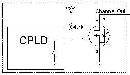
As shown in the above figure, to control a relay, you can connect one end of a relay coil to the Channel Out connection, and connect the other end of the coil to a power supply.
When a channel is not in use, the CPLD grounds the output for that channel. This shorts the gate of the FET (field-effect transistor) driver to the source, which turns off the FET and allows the drain to float. The coil of the relay pulls the drain up to the supply voltage, so there is no voltage drop across the coil and the relay is undriven.
When the CPLD drives a channel, it opens (tristates) the output for that channel. The FET gate and the CPLD open-drain output are both high impedance, so the pull-up resistor on the gate pulls the drain up to 5 V. This drives the FET into saturation and therefore holds the drain voltage to be just above the source voltage. Due to the voltage drop produced across the relay coil, the relay actuates.
Additional
User I/O & Pinout
Besides the relay driver channels and the return lines, the PXI-2567 provides triggers and power supplies at the front panel.
You can use the power supplies to control a limited number of relays. The PXI-2567 has a 5 V and a 12 V source available to drive relays. The 5 V source, available on pin 58, can provide up to 1.25 A of current. The 12 V source, available on pin 19, can provide 0.50 A of current.
Channel
Protection Circuitry
Each relay driver channel offers overtemperature, overcurrent, and overvoltage protection. These features are built into the FET drivers.
The built-in temperature sensor in each chip provides overtemperature protection. When the junction temperature exceeds 150 °C, the drain is automatically tristated. The chip automatically closes the drain when the temperature drops to 135 °C, as long as the gate of the FET driver remains high (enabled).
The overcurrent protection is based on the overtemperature protection. When the current exceeds the FET limit (over about 2 A continuously at 55 °C), the chip takes itself out of saturation. This increases the drain-source voltage, producing heat which increases the temperature above the 150 °C limit. The channel automatically opens, and the current path is broken.
The overvoltage protection has two parts. When the chip is on, the active logic in the driver bank IC monitors the gate voltage. When the gate voltage exceeds the specification, the circuitry automatically shunts current to reduce the voltage. This acts as flyback protection during typical relay driver use.
The chip also has a built-in Zener diode on the output. When the chip is not powered, this diode acts as flyback and provides overvoltage protection.
The driver bank chips are extremely durable, able to withstand high pulse currents and voltage shocks up to 16 kV on the drain. The overvoltage protection, which shunts current to reduce the voltage, can only shunt less than 100 mA continuously without fusing the drain to the source.
PXI-2567 Channel Diagram
The following figure shows the channel diagram of the PXI-2567.
