Chapter 1: Understanding Key RF Switch Specifications
Overview
This document is part 1 of the Guide to Selecting an RF Switch. This 5-part guide is an accumulation of insightful content that will arm you with the necessary knowledge to design your RF switch network. This section will explain basic RF switch specifications such as insertion loss, VSWR, characteristic impedance, and rise time.
For more information on NI's RF switch offering visit NI RF Switches main product page
Contents
- Introduction to RF Switching
- Characteristic Impedance
- Insertion Loss
- Voltage Standing-Wave Ratio (VSWR)
- Bandwidth
- Topology
- Isolation and Crosstalk
- Rise Time
- Conclusion
- Related Links
Introduction to RF Switching
With the recent surge in availability of RF switching products for test system development, choosing the right product for your application has become increasingly difficult. Most RF vendors describe their RF switching products using two main specifications – topology and bandwidth (such as the NI PXI-2594 2.5 GHz 4x1 multiplexer). While these specifications are indeed important and vital during the evaluation phase, they do not provide the buyer with enough information to make an informed purchasing decision. The goal of this tutorial is to introduce to you the following seven important specifications that must be considered when designing your RF switch network:
- Characteristic impedance
- Bandwidth
- Topology
- Insertion Loss
- Return loss and voltage standing-wave ratio (VSWR)
- Isolation and crosstalk
- Rise time
Before discussing characteristic impedance and other RF switch specifications, it is first important to understand the difference between how signals propagate in DC circuits versus RF systems. In DC circuits or circuits where the propagating signal has low frequencies, the voltage of the signal at different points on a cable in the signal path varies minimally. This is not so in the case of RF or high-frequency signals where wavelength of the signal is considerably small in comparison to the length of the cable allowing multiple cycles of the signal to propagate through the cable at the same time.
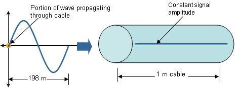
Consider an example where two waves (signals) of different frequencies are made to propagate through a 1 m coaxial cable. The frequency of the first signal is 1 MHz while that of the second signal is 1 GHz. To calculate their wavelengths, we will use the following formula:
In the above formula, l is the wavelength of the signal, f is its frequency, and VF is the velocity factor of the cable. Let us assume that the coaxial cable being used to route both signals is of type RG8, which is known to have a velocity factor of 0.66.
Then for
Signal 
Figure 1. A 1 MHz Sine Wave Propagating through a 1 m Coaxial Cable
In the case of Signal 1, the length of the coaxial cable is considerably small in comparison to the wavelength of the signal propagating through it. Therefore, as can be seen in Figure 1, the variation in potential of the signal at different points in the cable is negligible.
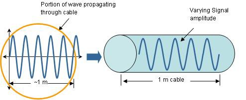
For Signal 2 where f = 1 GHz:
Figure 2. A 1 GHz Sine Wave Propagating through a 1 m Coaxial Cable
In the case of Signal 2, the length of the coaxial cable is much larger (almost 5X) than the wavelength of the signal propagating through it. Therefore, at any given time, multiple cycles of the signal will travel through the cable simultaneously. Because of their small wavelengths, high-frequency signals travel through cables in waves. Such signals therefore suffer reflections and power loss when traveling between varying media (wave theory). In the case of electrical circuits, this variation in medium takes place when the signal (wave) is made to pass through system components that have varying characteristic impedances. Therefore, to minimize reflections and power loss, RF systems must be constructed using suitable components with matched impedances. As a rule of thumb, signal degradation due to power loss and reflections that occur in the transmission line become significant once the length of the cable exceeds 0.01 of the wavelength of the signal it is being used to route.
Characteristic Impedance
Characteristic impedance is a transmission line parameter that is determined by the physical structure of the line. It also helps determine how propagating signals are transmitted or reflected in the line. Impedance of RF components is not a DC resistance and, in the case of a transmission line, can be calculated using the following formula:
Figure 3. Characteristic Impedance of a Transmission Line
In the above formula:
Z0 = Characteristic impedance
L = Inductance per unit length of the RF transmission line caused due to magnetic fields that are formed around the wires when current flows through them.
C = Capacitance per unit length of the RF transmission line. This is also the capacitance that exists between two conductors
R = DC resistance per unit length of the RF transmission line
G = the dielectric conductance per length
ω = frequency (radians/s)
Because an ideal cable has no resistance or dielectric leakage, its characteristic impedance can be calculated using the above formula as:
Because all components in an RF system have to be impedance matched to minimize signal losses and reflections, component manufacturers specifically design their equipment to have a characteristic impedance of either, 50 or 75 Ω. 50 Ω RF systems make up the bulk of the RF market and include most communications systems. 75 Ω RF systems are smaller in number and are prevalent mainly in video RF systems. It is crucial that engineers ensure that parts such as cables and connectors in addition to other instruments that may reside in the test system are all impedance matched.
Insertion Loss
Significant power loss in the signal occurs if the length of the transmission line it is made to propagate through is greater than 0.01 of its own wavelength. The “insertion loss” specification of a switch module is a measure of this power loss and signal attenuation. Insertion loss of a switch module at a particular frequency can be used to calculate the power loss or voltage attenuation caused by the switch on a signal at that frequency.
Formula for calculating power loss:
Formula for calculating voltage attenuation:
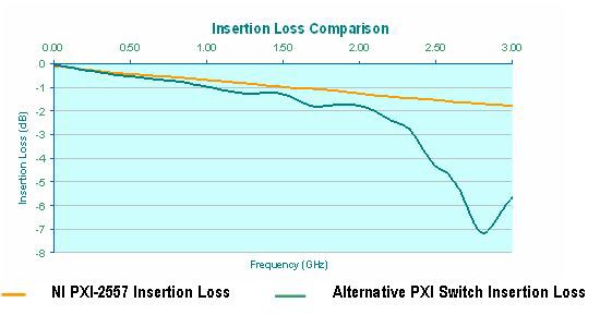
To understand the concept of insertion loss, think of a switch or relay as a lowpass filter. Every switch in the real world has some parasitic capacitance, inductance, resistance, and conductance. These parasitic components combine to attenuate and degrade the signal that the switch is being use to route. The power loss and voltage attenuation caused by these components varies with frequency of the input signal and can be quantified by the insertion loss specification of the switch module at that frequency. It is therefore critical to ensure that the insertion loss of a switch is acceptable at the bandwidth requirement of the application. To understand why this is important, let’s consider an example that compares the suitability of two switches for a particular RF application. The requirements of the application includes routing eight 3 GHz video signals to a channel on a vector network analyzer with less than 30 percent attenuation (insertion loss should be less than 3 dB at 3 GHz). The first switch being considered is the NI PXI-2557 75 Ω 2.5 GHz 8x1 multiplexer while the second is a 3 GHz 75 Ω 8x1 multiplexer from another PXI vendor. Upon preliminary examination of the higher level specifications of both modules, it appears that the latter would be more suitable (the latter has a better bandwidth specification). However, a closer inspection of both products reveals that this hypothesis does not hold true. The following graph displays insertion data from 160 MHz to 3 GHz collected on both switch modules.
Figure 4. Insertion Loss Comparison for Switch Modules from Vendors A and B
As can be seen, at 3 GHz, insertion loss of the 2.5 GHz module is approximately 1.78 dB while that of the 3 GHz switch is closer to 5.64 dB. From these values we can calculate the subsequent voltage and power loss caused by both modules to be:
| NI PXI-2557 | Other PXI Vendor | |
| % Voltage Attenuation at 3 GHz | 18.3 | 47.8 |
| % Power Loss at 3 GHz | 33.3 | 72.7 |
Table 1. Voltage and Power Loss Percentage Comparisons
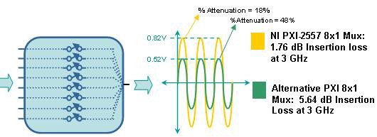
The values from the above table indicate that a 3 GHz 1 Vpp sine wave, when made to pass through the NI PXI-2557 2.5 GHz 75 Ω multiplexer, would be attenuated to 0.817 Vpp. The same signal when made to pass through the 3 GHz 75 Ω multiplexer from the other PXI vendor will be attenuated to 0.522 Vpp. Thus it can be seen that even though the bandwidth specification of the switch module from the alternative PXI vendor is higher than that of the NI module, the net signal degradation caused by it is significantly higher than that caused by the NI PXI-2557. Furthermore, it is safe to say, that in the case of the aforementioned 3 GHz application, the 2.5 GHz NI switch module is a better fit than its 3 GHz counterpart.
Figure 5. Comparison of Attenuation Caused on a 1 Vpp Sine Wave
Voltage Standing-Wave Ratio (VSWR)
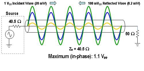
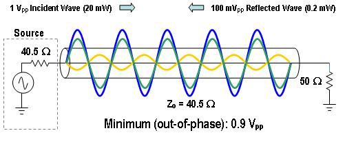
VSWR is the ratio of reflected-to-transmitted waves. As mentioned earlier, at higher frequencies, signals take the form and shape of waves when passing through a transmission line or cable. For this reason, just as in the case of sound and light waves, reflections occur when the signal traverses over different media (such as components with unmatched impedances). In a switch module, this mismatch can be between the characteristic impedance of the connector, the PCB traces, and the actual relay itself. Because VSWR is a measure of the power of the reflected wave, it can also be used to measure the amount of power loss in the transmission line. The reflected wave, when summed with the input signal either increases or decreases its net amplitude, depending on whether the reflection is in phase or out of phase with the input signal. The ratio of the maximum (when reflected wave is in phase) to minimum (when reflected wave is out of phase) voltages in the "standing wave" pattern is known as VSWR. To understand how to calculate VSWR and return loss in an RF system, let us consider the RF transmission line shown in Figure 6.
Figure 6. Comparison of Attenuation Caused on a 1 Vpp Sine Wave
In the circuit in Figure 6, the impedance of the load (40.5 Ω) is not equal to that of the source and the transmission line (50 Ω). For this reason, some portion of the signal propagating through the transmission line is reflected back from the load. We can measure this reflection using the following formula:
As you can see, return loss is a measure of the power of the reflected signal. It is also a subset of insertion loss. The higher the return loss (or reflections) in an RF system, the higher its insertion loss.
VSWR is another way of measuring signal reflections. It can be calculated as:
In the above formula, G is the reflection coefficient and can be calculated using the following formula:
For the circuit in Figure 6, we calculate VSWR to be:
To visualize what is happening in this example, let us imagine that the signal being sourced in the RF system is a 1 Vpp sine wave. Because the reflection coefficient for the system is 0.1, we can determine that the magnitude of the reflected is 0.1 x 1 = 0.1 V or 100 mV. Figure 7 displays the maximum and minimum amplitudes of the resultant signal which occurs when the reflected wave is in phase and 180 deg out of phase with the input signal, respectively.
Figure 7. Maximum and Minimum Voltages in the Standing Wave
As stated earlier, VSWR is the ratio of maximum voltage to minimum voltage in the standing wave pattern. Using this definition, we can calculate VSWR from Figure 7 to be:
Bandwidth
As mentioned before, bandwidth of a switch module is one of its main specifications. However, bandwidth provides us with only an approximation of the performance of a given product, because the process of establishing a bandwidth specification for an RF switch varies between vendors. The bandwidth of a switch simply indicates the maximum frequency signal that the vendor believes can be routed through it with acceptable loss. But, what is acceptable for one vendor may be unacceptable for another. Hence a 3 GHz switch for example from Vendor A may have completely different performance metrics than a 3 GHz switch from Vendor B.
Consider again the example of two modules made from different vendors with similar topology and characteristic impedance but different bandwidth specifications. The first module, the NI PXI-2557, is a 2.5 GHz 8x1 multiplexer with 75 Ω characteristic impedance; the switch from the alternative PXI vendor is a 3 GHz 8x1 multiplexer with 75 Ω characteristic impedance. Though it may seem that the second module is better suited for routing signals between 2 and 3 GHz, insertion loss data collected and displayed in Figure 3 indicates otherwise. For this reason, the bandwidth specification of the NI module is far more conservative than its counterpart.
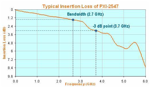
Bandwidth of a product is also thought, by many, to be its -3 dB bandwidth. This viewpoint is accurate for instruments such as digitizers where the bandwidth specification of the device is in fact the -3 dB point of the analog front end of the instrument. However, for an RF switch, the relation between bandwidth and -3 dB does not always hold true. While some vendors do in fact specify bandwidth at -3 dB, others do not. An example of this can be seen from the graph in Figure 8, which shows insertion loss of the NI PXI-2547 at its bandwidth (2.7 GHz) in conjunction with its -3 dB point (3.7 GHz).
Figure 8. Insertion Loss of the NI PXI-2547 2.7 GHz 50 Ω 8x1 Multiplexer
Topology
Topology is one of the most important features to consider when choosing an RF switch. Picking a switch with the wrong topology can cause considerable effects on insertion loss and VSWR. The two main types of topologies available for RF are multiplexers and single-pole double-throw (SPDT) relays. A multiplexer is a switching system that sequentially routes numerous inputs to one output or vice versa. An SPDT relay is a scaled down version of a multiplexer. A single SPDT relay can route two inputs to one output or vice versa. RF multiplexers are often made up of multiple SPDT relays.
Different applications require differing mixes of RF switch topologies. For example, to conduct a stimulus-response test on a 4-channel device under test (DUT), you can use a module with two individual 4x1 multiplexing banks. On the other hand, for a test that conducts analysis from the outputs of eight individual DUTs, a module with a single 8x1 bank would be preferable. Due to the availability of several RF switches on the market, it is important to understand the optimum uses for these various topologies to pick the best option for your application.
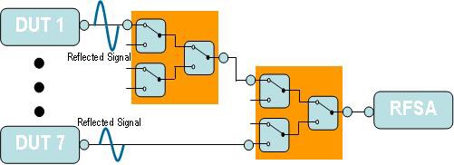
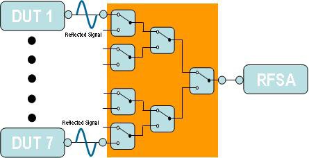
By discussing two varying approaches to building a 7x1 multiplexer, the example in Figures 9 and 10 will demonstrate why one is preferable. The first approach cascades two 4x1 multiplexers to build a single 7x1 multiplexer. The disadvantage of this setup is that it requires that a signal from a DUT pass through two switch modules (four SPDT relays in total) before reaching the vector network analyzer (VNA). Therefore the net insertion loss that occurs in the signal path is now the sum of the individual insertion loss specifications of each individual relay and cables in the system.
Figure 9. Two Cascaded 4x1 Multiplexers
The second approach uses an inherent 8x1 multiplexer (such as the NI PXI-2547 50 Ω 2.7 GHz 8x1 multiplexer) to route seven DUTs to the VNA. This configuration will improve system insertion loss not only because it reduces the total number of SPDT relays in the signal path (three SPDT relays instead of four) but also because it eliminates additional wiring in the system such as the cables that exists between modules in the previous system. Thus, the quality of the signal reaching the VNA in the second system is likely to be far better than that of the first.
Figure 10. An 8x1 multiplexer topology uses fewer relays to route a signal than two 4x1 multiplexers.
For more information on choosing a switch with the best suited topology for your application, read Chapter 2 in The Guide to Selecting an RF Switch.
Isolation and Crosstalk
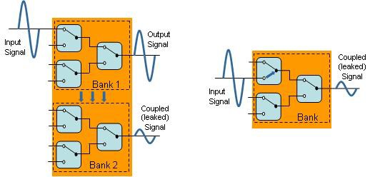
Isolation is defined as the magnitude of a signal that gets coupled across an open circuit. Crosstalk is defined as the magnitude of a signal that is coupled between circuits (such as separate multiplexer banks on an RF module).
Figure 11. Crosstalk versus Isolation.
Rise Time
If a signal is purely sinusoidal, the bandwidth/insertion loss performance of a switch module is sufficient to determine whether the product fits the application. However, for signals that have multiple frequency components, such as square waves, this may not be as simple because maintaining the integrity of such signals depends on the impact the switch will have on signal rise time. Because a square wave is made up of a number of sine waves that vary in frequency, to get an accurate measurement, the bandwidth of the switch must be high enough to cause minimum attenuation on all individual sine waves. As a rule of thumb, for a square wave, once the 5th or 7th harmonic is reached, the change in the rise time is minimal. Therefore, in general a square wave can be routed through a switch if the -3 dB point of the switch (frequency at which point insertion loss equals 3 dB) is 7X the fundamental frequency of the square wave. Some vendors specify the rise time of the switch. If this case, check to make sure that the rise time specification of the switch module is less than the rise time of the highest harmonic that needs to be routed with minimum distortion.
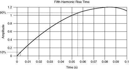
The figure below displays the rise time measurement for the 5th harmonic of a square wave. Let’s assume that this is the highest harmonic of the square wave that needs to be routed through the switch. To determine whether a particular switch can successfully route the signal, we need to compare the rise time of the switch with the rise time of the harmonic. Sometimes this specification is not available for a switch module. In such cases, we can calculate the -3 dB point of this harmonic and compare it with the -3 dB point of the switch. -3 dB point can be calculated from rise time using the formula:

Figure 12. Fifth Harmonic of a Square Wave
For the signal in shown in above figure we calculate frequency at which -3 dB is reached to be 6.36 Hz (rise time is 0.055 s). Therefore, a switch for which insertion loss is less than 3 dB at 6.36 Hz or higher will be sufficient to route the square wave.
Conclusion
The voltage specification of an instrument or switch is a physical limitation of that device. Similarly, the sampling rate of a digitizer and the accuracy of a digital multimeter describe well the maximum capability of the instrument. A 200 MS/s digitizer cannot achieve a real-time sample rate faster than 200 MS/s. However, a 2 GHz RF switch can route signals above 2 GHz, but with more power loss. For this reason, selecting the best and most cost-effective RF switch for your application requires a thorough review of the datasheet of the product to determine whether its insertion loss, VSWR, isolation, and other specifications meet the requirements of your system. Some vendors provide sweep charts to display these specifications for an entire range of frequencies, while others will only provide specifications for a particular frequency. In such cases, it is important to contact the vendor and obtain more complete specifications to determine if the product is suited for your application.

