Introduction to Using DRAM with NI FPGA Devices
Overview
Contents
Using DRAM
The native LabVIEW FPGA interface to DRAM is through memory items. This interface gracefully abstracts away the low-level complexity of communicating with the physical DRAM on the device, arbitrating competing requests for DRAM resources, and segmenting the memory for maximum usage flexibility. The result is a simple interface to write to and read from DRAM.
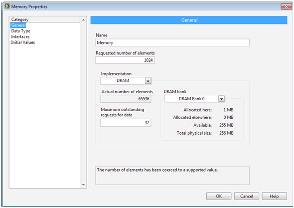
DRAM memory items are created globally in the Project Explorer. To create a DRAM memory item, right-click on your FPGA target and select New»Memory. Then, select “DRAM” for the implementation. A memory item targets a single DRAM bank and, provided that there are no other memory items allocated to the selected DRAM bank, can be as large as the entire bank.
Figure 1. Use the Memory Properties window to configure the DRAM memory item size, data type, and DRAM bank.
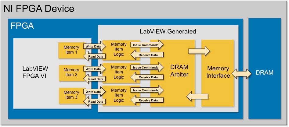
You can also segment the full DRAM space into smaller memories that can be accessed independently from different sections of the LabVIEW FPGA code by creating multiple memory items that use the same DRAM bank. LabVIEW automatically handles the arbitration code and gives all of the resulting interfaces equal access to DRAM. The figure below shows the logic that LabVIEW generates to provide access to a given DRAM bank.
Figure 2. LabVIEW has built-in arbitration schemes to handle multiple interfaces to DRAM.
Write Method
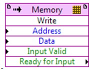
To store data in DRAM, use the Write method shown below. It takes an address to write to and the data to store in that address. The handshaking terminals, Input Valid and Ready for Input, are used to ensure that only valid data is written to memory. The write command is pushed to the interface when a value of true is written to the Input Valid input. The Ready for Input terminal indicates if the interface is ready to accept new data. If Ready for Input is false, the data is ignored and a write command is not written. To avoid information loss, make sure to only push data into the write method when Ready for Input is true.
Note: Follow best practices for out of range accesses. Reading or writing to addresses beyond the size of your memory block can have very confusing behavior. Always be mindful of how many elements are allocated to your memory block. By enabling error terminals on your memory methods, you can detect out of bounds memory accesses.
Figure 3. Use the memory item write method to write data to DRAM.
Read Methods
To retrieve data from DRAM, you use two method nodes: Request Data and Retrieve Data. The first method node, Request Data, uses the address of the data that you are interested in to request the data at that address from the memory controller. However, DRAM has relatively long latency on top of the requirements of arbitration and nondeterministic occurrences such as a DRAM refresh. Therefore, data is not immediately available. Rather, requests are queued up and processed in the order received. After some time has elapsed, the Retrieve Data method outputs the next piece of data asked for and asserts the Output Valid to indicate that data is available. Data is returned only if the Ready for Output terminal is set to true, as this indicates to the memory interface that the downstream logic is ready to receive the data.
Note: Follow best practices for out of range accesses. Reading or writing to addresses beyond the size of your memory block can have very confusing behavior. Always be mindful of how many elements are allocated to your memory block. By enabling error terminals on your memory methods, you can detect out of bounds memory accesses.
Figure 4. Use the request data to initiate a request for data and the retrieve data method to get the data.
Supported Devices
| Number of DRAM Banks | Size per Bank | Bandwidth per Bank | ||
|---|---|---|---|---|
| R Series Devices | ||||
| PXIe-7821R | 1 | 512 MB | 800 MB/s | |
| PXIe-7822R | 1 | 512 MB | 800 MB/s | |
| FlexRIO FPGA Modules | ||||
| PXI-7952R | 2 | 64 MB | 800 MB/s | |
| PXI-7953R | 2 | 64 MB | 800 MB/s | |
| PXI-7954R | 2 | 64 MB | 800 MB/s | |
| PXIe-7962R | 2 | 256 MB | 1.6 GB/s | |
| PXIe-7965R | 2 | 256 MB | 1.6 GB/s | |
| PXIe-7966R | 2 | 256 MB | 1.6 GB/s | |
| PXIe-7972R | 1 | 2 GB | 10.5 GB/s | |
| PXIe-7975R | 1 | 2 GB | 10.5 GB/s | |
| PXIe-7976R | 1 | 2 GB | 10.5 GB/s | |
| PXIe-7912* | 2 | 2 GB | 8.5 GB/s | |
| PXIe-7915* | 2 | 2 GB | 8.5 GB/s |
* These values apply to FlexRIO Integrated I/O Modules based on the same FPGA as the corresponding coprocessor. For instance, the PXIe-7915 values apply to all Integrated I/O Modules with a KU060 FPGA.


