Chapter 4: Effects of Impedance Matching and Switch Quality on RF Test System Performance
Overview
This document is part 4 of the Guide to Selecting an RF Switch. This 5-part guide is an accumulation of insightful content that will arm you with the necessary knowledge to design your RF switch network. This section will highlight the importance of impedance matching in RF systems using graphs and circuit diagram analysis. Please see the related link section below to navigate to the first page of the guide.
For more information on NI's RF switch offering visit NI RF Switches main product page.
Contents
- Introduction
- Characteristic Impedance
- Reflected Power due to Impedance Mismatches
- Impedance-Matched Switches
- Related Links
Introduction
Switch systems can be used to increase channel count and automate signal routing in test systems ranging from precision DC measurements to RF. However, the characteristics and design of a switch module that will work for DC measurements versus those of a product best suited for RF systems are vastly different. Switches designed for higher frequency systems typically have lower channel count than their low-frequency counterparts due to increased relay size and larger isolation (spacing) requirements and can be considerably more expensive. What properties do switches marketed as ‘RF’ or ‘High Frequency’ have that are not present in those used for lower frequency applications? The answer lies in the careful attention to characteristic impedance throughout the switch design.
This chapter will begin by defining characteristic impedance and the importance of impedance matching in RF switch systems. Impedance matching is designing an RF system so that all the source, load, and characteristic impedances match, in order to ensure maximum power transfer and minimum reflected power. It will then proceed to elaborate on design considerations for switch products and networks to improve impedance matching in switch systems and minimize signal reflections and power loss.
Characteristic Impedance
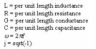
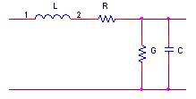
Any RF transmission line, of which all coaxial cables and switches are a subset, has some characteristic impedance that may or may not be constant over the length of that line. Characteristic impedance can be defined along any point on that transmission line as the ratio of a single pair of voltage and current waves at that point in the cable in the absence of all reflections. Practically speaking, frequency and the per unit resistance, conductance, capacitance, and inductance of a line will determine the ratio of voltage and current, and will thus also define characteristic impedance, which is usually denoted Zo.

Figure 1: Lumped Model of a Very Short Segment of Transmission Line
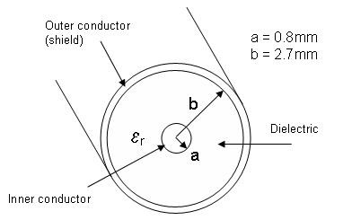
Cables with common geometries such as coaxial cables have very little variation in characteristic impedance across their lengths. It is therefore easy to calculate their characteristic impedance. For example, consider the coaxial cable shown in Figure 2.
Figure 2: Example Coaxial Cable
To calculate the characteristic impedance of the coaxial cable shown above, the following equation can be used:
In the above equation
You can also measure characteristic impedance throughout the length of a transmission line using a time-domain reflectometer (TDR) by connecting it to one end of the cable and using it to emit a pulse with a very fast edge rate down the cable and then measuring the reflections caused by any impedance changes in the cable. Using the TDR, you will find that the largest reflection in the transmission line occurs at the end of the cable when it is left as an open circuit, because the instrument is actually measuring the very large resistance between signal and ground at the end of the cable. Terminating the line with its characteristic impedance will result in a line that looks infinitely long because there are no reflections coming from the end of the cable. TDR techniques are also used to locate faults (opens or shorts) in cables, which appear as either very high or very low characteristic impedance.
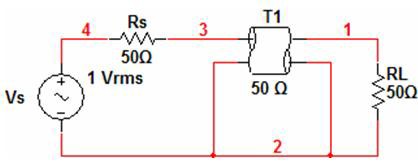
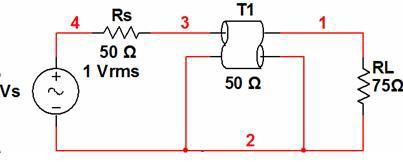
In most RF systems, it is desirable to transfer as much power as possible from source to load. To ensure this happens, the source and load impedances should be matched, and the transmission line used to connect the two should have an equal characteristic impedance as well.
Figure 3: System with Perfect Impedance Matching
Any mismatch in the impedance of these three components in an RF system will cause a portion of the signal power traveling from source to load to be reflected back to the source. The magnitude of the mismatch will determine the portion of the power that keeps traveling down the cable towards the load and the portion that gets reflected back to the source.
Figure 4: Impedance Mismatch at RL
Because impedance matching between components is imperative to performance in an RF system, the RF market has standardized on several characteristic impedances, the most popular of which are 50 and 75 Ω. This fact has permitted vendors of RF equipment (instruments, switching, and cabling) to design their components specifically for either 50 or 75 Ω systems. Most RF test and measurement equipment manufactured today has a characteristic impedance of 50 Ω. Such equipment is best suited for communications applications, which make up the bulk of RF applications. On the other hand, 75 Ω products are best suited for applications that involve transmitting or routing video signals (e.g. NTSC and PAL).
Characteristic impedances for coaxial cables were standardized in order to optimize one parameter or another in the cable, such as lower loss or power handling ability. For an air dielectric, maximum power handling occurs near 30 Ω, while minimum loss occurs around 75 Ω. Filling the cable with a dielectric other than air will have an effect on the frequency at which maximum power handling and minimum loss occur.
Reflected Power due to Impedance Mismatches
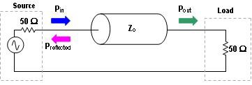
We have discussed the importance of impedance matching in RF systems. This section of the tutorial will elaborate on what happens when characteristic impedances of components in such systems are not matched. In the system depicted in Figure 5, an RF source is connected to a load via a transmission line that has a characteristic impedance of ZO. Some of the power traveling into the line makes it out the other side (Pout), some is dissipated in the resistance and conductance of the cable itself, and some is reflected back to the source (Preflected).
Figure 5: Illustrating Power Flow for a Simple Circuit
One measure of the amount of reflected power is return loss, which is a logarithmic ratio of the power of the signal reflected back to the source to the power output by the source. Values for return loss range from infinity, for a perfectly matched system, to zero for open or short circuits. Some signal sources are sensitive to power being reflected back to them and require an overall system performance with lower return loss designed to minimize impedance discontinuities and signal reflection. Return loss can be calculated using the following formula:
To understand reflection loss better, let us assume that the output power of the source is constant. In such a case, an increase in power of the signal reflected back to the source would cause a corresponding decrease in power of the signal that arrives at the load. Again, because variations in characteristic impedances of components within the system are what cause such signal reflections, it can be deduced that systems with poor impedance matching will experience more return loss than well matched systems.
VSWR (voltage standing-wave ratio) is another measure of impedance matching and reflected power in an RF system. As its name implies, VSWR is calculated by taking the ratio of the largest to the smallest amplitude values of the standing wave created by the combination of the incident and reflected waveforms. Values of VSWR range from one for a perfect impedance match to infinity for an open or short circuit.
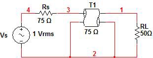
A simple example using a single impedance discontinuity will be used to illustrate VSWR. In the circuit shown in figure 6, an incident wave traveling in a 75 Ω coaxial cable will encounter a 50 Ω termination. When this occurs a portion of that signal will be reflected back causing a standing wave. The location of the impedance discontinuity will be at distance x=0.
Figure 6: Single Impedance Discontinuity
The reflection coefficient (denoted as G) can be calculated using the following formula:
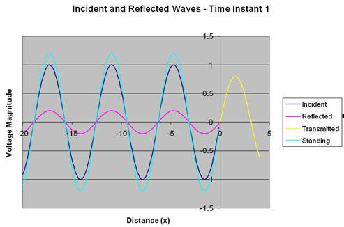
At one particular instant in time, the waveforms will look like those shown in Figure 6 below. The source is set to output a 1 Vpp sine wave. This particular scenario shows the largest possible magnitude of the standing wave because both the incident and reflected waves are in phase (the standing wave has an amplitude that is the vector sum of the incident and reflected wave). In Figure 7, it can be seen that the amplitude of the standing wave (in light blue) is 1.2 Vpp, which is the sum of amplitudes of the original signal (1 Vpp) and the reflected wave (0.2 Vpp)
Figure 7: Voltage Waveforms at Time Instant 1
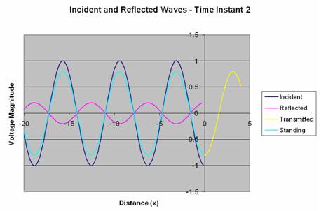
The smallest possible standing wave must then occur when the incident and reflected waves are 180 deg out of phase. Figure 8 shows the behavior of all four waveforms at this time instant. You will notice that the amplitude of the standing wave is 0.8 V (amplitude of the original signal minus the amplitude of the standing wave)
Figure 8: Voltage Waveforms at Time Instant 2
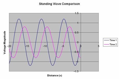
If the standing waves for both time instants are put on the same graph, the magnitude difference is easy to see.
Figure 9: Standing Waveforms from Both Time Instants
To calculate VSWR for this interface, simply take the ratio of the largest standing wave to the smallest standing wave. In this case:
Because VSWR and return loss are two ways to measure the same property, you can use the following equations to convert between the two:

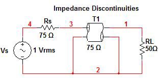
To understand these theoretical concepts better, let’s consider a practical example system in which a source and load with 50 Ω termination impedances will be connected to each other via a 1 m 75 Ω coaxial cable. The two impedance discontinuities in this system will both cause power to be reflected back to the source.
Figure 10: Circuit with Two Impedance Mismatches
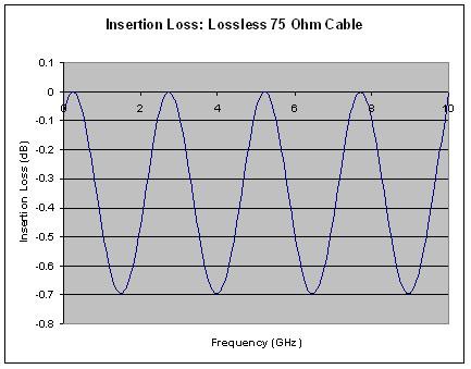
If the transmission line is initially assumed to be lossless, the graph in Figure 11 shows that there is as much as 0.7 dB of insertion loss due exclusively to the reflections caused by the two impedance discontinuities. Recall that when power gets reflected back to the source it can never make it to the load, therefore this reflected power must also cause an increase in insertion loss, which is based on how much power makes it to the load. The distance between peaks and valleys in the graph is directly related to the length of cable used.
Figure 11: Insertion Loss due only to Power Reflection
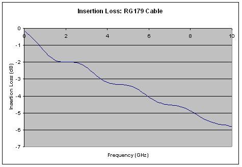
For a cable model including conductive and resistive losses in the cable, Figure 12 shows the insertion loss performance of the system. The slope of the line is mainly due to conductive and dielectric losses in the cable, and the ripple is due to variation of return loss over frequency (as much as 0.7 dB in this example).
Figure 12: Total Insertion Loss for the Circuit in Figure 9
Impedance-Matched Switches
Although most of the previous discussion and examples involved cables, impedance matching in switching modules, which are used to expand channel count in RF test systems, is equally important for the same reasons. Impedance through a switch module will vary more than for a cable due to differences in the various components that must be combined to construct the signal path, such as relays, connectors, and PCB traces. Because design and components used in an RF switch module vary so much from one vendor to another, it is very important to carefully inspect the VSWR of the product (to obtain data about potential signal reflections) and insertion loss when deciding whether it will fulfill the needs of your test system.
To ensure good performance at higher frequencies, a good RF switch has components and design that minimize impedance mismatches and keep insertion loss and reflections to a minimum. For this reason, choosing quality components to build the switch has a huge impact on performance.
Relays
One of the most significant factors in the overall performance of a switch module is the choice of relays for internally routing signals. For switches commonly used in ATE systems, two relay types are generally used – PCB-mount relays and coaxial switches.
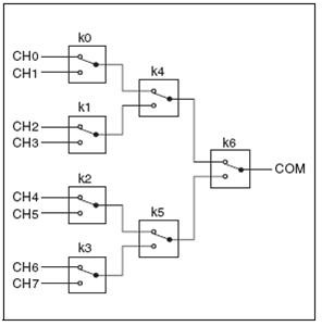
PCB-mount relays are available in several configurations such as Form C (SPDT). You can use multiple SPDT relays on a PCB to create larger topologies such as multiplexers (SP4T and up) or matrices. Figure 13 shows how an 8x1 (SP8T) multiplexer configuration is created using SPDT relays.
Figure 13: 8x1 Multiplexer Topology Created from Form C Relays
Several vendors produce parts that can be used for this purpose, with some models having acceptable performance up to several GHz. Because the relay leads are soldered to PCBs, it is up to the manufacturer of the switch module to interface I/O connectors to the relays in an impedance-controlled manner. For this reason, switch manufacturer design expertise plays a major role in designs that use these PCB-mount devices. Although the internal impedance of the relays cannot be changed, techniques are available by which designers can minimize the effect of reflections caused by impedance discontinuities.
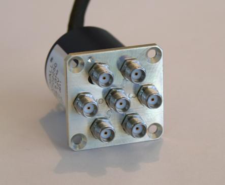
The other type of relay commonly used in RF switching modules is the coaxial or ‘can’ type. Coaxial switches include the entire RF transmission path in their mechanical enclosure and have coaxial connectors for directly interfacing to RF test signals. Figure 14 shows a photo of an example coaxial switch. A completely coaxial (and impedance-controlled) design results in performance up to 40 GHz for some models, an order of magnitude improvement over PCB relay designs. Insertion loss performance of a coaxial switch module is typically better than that of PCB-mount relay designs, but the cost is substantially higher than PCB-mount relays and the devices typically occupy a much larger space. RF performance of this type of switch module will depend mostly on the relay manufacturer and not the module designer. The NI PXI-2596 is an example of a switch module made with coaxial switches manufactured by Radiall.
Figure 14: Coaxial Switch
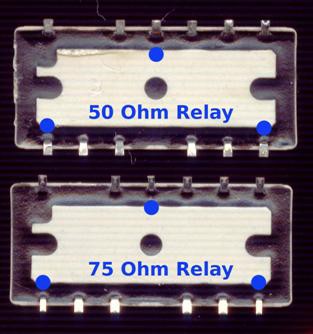
PCB-mount relays that are marketed for use in RF systems are designed for either 50 or 75 Ω characteristic impedance. Some manufacturers even offer parts for either impedance in identical package types. In such designs, the internal relay design geometry must change to meet the impedance requirements. Figure 15 illustrates the pinout difference of 50 and 75 Ω versions of Omron G6Z series relays, which are available in a number of terminal configurations. Note how the size of the leads for the RF signal path (marked with blue dots) is slightly smaller in the 75 Ω version of the part, producing a higher characteristic impedance.
Figure 15: Terminals of Similar 50 and 75 Ω Relays
Using 50 Ω relays in 75 Ω switch modules and vice versa will have the same overall system effect as the previous example where a 75 Ω cable was used in a system with 50 Ω source and load terminations.
Connector Type
In PCB-mount switch designs, connector type and trace geometry will also affect overall module performance. The highest frequency at which a module will need to operate will determine the connector type used for I/O signals. For many 50 Ω applications, this connector type is SMA, which offers consistent performance in a small area. The SMB connector, also popular for switch modules rated less than 4 GHz, is easier to mate than the SMA due to a press-on interface; the two connectors are pressed together rather than screwed together.
PCB Traces
PCB trace impedance will depend on the geometry of the copper and dielectric used. The most common types of transmission line used in PCB construction for switch modules are microstrip, stripline, and coplanar waveguide. Each type has strengths and weaknesses. For example, the stripline will have much better isolation performance than microstrip, but because there must be a ground plane above and below the signal trace, vias are required in the signal path. Vias can be more difficult to impedance match. Coplanar waveguides offer the ability to change the width of the trace to an extent without effecting characteristic impedance (the width of the gap to ground must also be changed).
In PCB-mount relay module designs, isolation (a measure of how much signal leaks from one channel to the next) is determined by relay performance, board layout, and shield effectiveness. Without adding additional relays in the signal path (which are usually referred to as ‘isolation relays’), the absolute best isolation performance possible for a module is determined by the isolation of the relays used. Interaction between traces on the PCB due to poor board layout or inadequate shielding will further degrade the isolation specifications of the module. Board layout and shielding are also the two primary factors in crosstalk performance when a module has multiple banks on a single PCB.
