Chapter 2: Optimizing the Design of Your RF Switch Network
Overview
This document is part 2 of the Guide to Selecting an RF Switch. This 5-part guide is an accumulation of insightful content that will arm you with the necessary knowledge to design your RF switch network. This section will discuss the importance of switch system design by explaining how choosing the right topology for your application can increase its performance incrementally. Please see the related link section below to navigate to the first page of the guide.
For more information on NI's RF switch offering visit NI RF Switches main product page.
Contents
- Introduction
- RF Switch Topologies
- Choosing the Right Topology for Your System
- Example: Designing a 7x1 multiplexer
- Related Links
Introduction
The previous chapter discussed how and why signal degradation occurs in high-frequency signals. It also discussed the two main reasons for this degradation: power dissipation in the line, and power loss due to reflections in the transmission line. However all discussions and explanations thus far have been made from a single module perspective. In a typical RF system, the switch network consists of multiple modules and cables. These networks may be constructed in numerous arrangements with modules of varying topologies. To understand the how to design the best arrangement for your RF system, it is important to understand the different RF switch topologies.
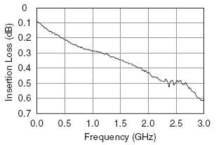
Before discussing available topologies and the effects they have on the insertion loss and voltage standing-wave ratio (VSWR) specification of the system, let’s recap the key concepts from the previous chapter. Insertion loss is a cumulative measure of total power loss that takes place in the line. It is the logarithmic ratio of the power of the signal that leaves the transmission line to the power of the signal that enters the transmission line. Voltage attenuation and power loss that a transmission line will cause on a signal of a particular frequency can be calculated using its insertion loss specifications. The following graph, which can be found in the specifications document of the NI PXI-2548 Quad SPDT Relay module, displays its insertion loss performance.
Figure 1. Insertion loss performance of the NI PXI-2548
Using data from this graph we can deduce the power loss and voltage attenuation that the switch will cause on a 2 GHz 1 Vp-p 1 W sine wave to be:
Power loss:
Voltage attenuation:
Therefore power loss in the above signal when it is made to pass through the NI PXI-2548 is 0.09 W and voltage attenuation is 0.046V.
Voltage standing-wave ratio or VSWR is another specification often listed in the datasheet or specifications document of an RF switch. VSWR is a measure of signal reflections that occur in a switch module due to impedance mismatches.
Because VSWR and insertion loss cumulatively provide information about the net degradation that a transmission line will cause on a signal, they are both important specifications to consider when choosing the right product for your application. However, knowing the VSWR and insertion loss of an RF switch is sometimes not enough. RF systems often require intricate switching networks to route signals from one point to another. These networks are usually comprised not only of a number of RF switches that may vary in topology but also of connectors and cables with varying lengths. Therefore in order to minimize of signal degradation in an RF application it is important to design an efficient switch system. Doing so requires in depth knowledge of RF switch topologies and how they can be combined to build switch networks.
RF Switch Topologies
The two main types of RF switch topologies that exist are multiplexers and general-purpose relays. Together these two kinds of RF switches can be combined to build large intricate switch networks.
General-purpose RF relay modules are usually made up of Form C (SPDT) relays and are usually used to route a signal between 2 places. For example, if a signal needs to be analyzed using an RF analyzer and then broadcasted to multiple locations through an antenna, it can be routed to both locations using a single SPDT relay.
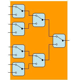
Multiplexers are devices that route several inputs to a single output or vice versa, sequentially. Multiplexers are ideal for increasing the channel-count of complex and expensive instruments such as RF analyzers and generators. One example of where a multiplexer would be useful would be on the production floor to test the functionality of a mass produced RF device such as a cell phone. Let’s assume that these devices are tested in batches of 100. In this case, it would be cost-prohibitive to dedicate an RF analyzer for the testing of each individual cell phone as this would require 100 RF instruments which could cost anywhere from a couple of thousand to a few hundred thousand dollars each. Another way to conduct this test would be to manually route all 100 devices one at a time to a single RF instrument. Although this route would be more affordable than having multiple RF instruments, it would increase test times significantly. The best test set up for this particular manufacturer would be to build an automated RF test system that uses a 100x1 multiplexer to automatically route 100 cell phones to the RF analyzer which takes a measurement and stores it in an appropriate manner using software.
In general, multiplexers can be built using multiple SPDT relays. For this reason, it is common for multiplexers to have higher insertion loss than their SPDT counterparts because the insertion loss of a multiplexer is the sum of the insertion loss of the individual SPDT relays that are contained inside it as well as the insertion loss of the PCB trace that routes the signal between these SPDT relays.

Figure 2. NI PXI-2548 50Ω 2.7 GHz Quad SPDT Relay Module and NI PXI-2547 50Ω 2.7 GHz 8x1 Multiplexer
As can be seen, in the above figure, the number of SPDT relays that a signal has to pass through in the PXI-2548 general-purpose RF switch module is one. Hence the insertion loss of this module is almost equal to the insertion loss of the SPDT relay itself. However, in the case of the PXI-2547, the signal has to travel through 3 SPDTs as well as the PCB traces that connect these SPDTs together. Hence the insertion loss of the PXI-2547 will be more than three times the insertion loss of each individual SPDT relay.
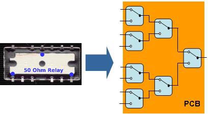
There are a variety of off-the-shelf RF general-purpose and multiplexer switch modules available in the market today. These off-the-shelf solutions are either constructed using coaxial switches more commonly known as ‘cans’, or using Printed Circuit Board (PCB) relays. Coaxial switches or ‘cans’ include the entire RF transmission line in their mechanical enclosure. On the other hand, modules built using Form C (SPDT) PCB relays use PCB traces to connect between individual relays which are soldered to the PCB. Although RF switch modules built using PCB relays cost less, they often have higher insertion loss and VSWR specifications than coaxial switches because they use multiple components (i.e. multiple SPDT relays, PCB traces, solder, etc.) to route inputs to a single output.
Figure 3. 6x1 multiplexer created using coaxial switches or ‘cans’
Figure 4. 8x1 multiplexer built using seven Form C (SPDT) relays
Choosing the Right Topology for Your System
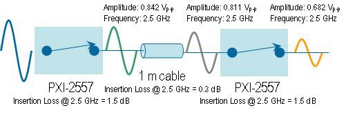
As demonstrated above, the more indirect the signal path, the greater the insertion loss in the transmission line. This concept does not only pertain to each individual switch module but to the switch system as well. Consider an example in which a 16x1 multiplexer has been built by cascading 2 PXI-2557 75Ω 2.5 GHz 8x1 multiplexers. The insertion loss for this switch network would then be the sum of the insertion loss of each individual PXI-2557 (which in turn is the sum of the insertion loss of SPDT relays and PCB traces that are used to construct the PXI-2557) and the insertion loss of the cable that is being used to connect them together. Figure 5 illustrates this concept.
Figure 5. Insertion loss increases with increase in components in signal path
Hence, in order to minimize insertion loss in a system, the switch network must facilitate the shortest possible signal path.
Example: Designing a 7x1 multiplexer
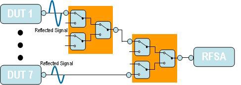
Method 1: Cascading 2 4x1 Multiplexers
Figure 6.Cascading 2 4x1 multiplexers to create a 7x1 multiplexer
One method of building a 4x1 multiplexer is by cascading two 4x1 multiplexers by connecting the COM of the first multiplexer to an input channel on the second one. This design has some major flaws that could cause serious discrepancies in measurements and test results. Perhaps the biggest disadvantage of this design is the fact that the length of the signal path varies from channel to channel. For example, a signal from Device Under Test (DU1) 1 has to pass through 4 SPDT relays before reaching the RF signal analyzer. Therefore, the loss in the signal path for DUT 1 will be the sum of the loss that will occur in all 4 SPDT relays and the cable that connects the two individual modules. On the other hand, the signal from DUT 7 will only have to pass through 2 SPDT relays and will hence suffer much less loss. In addition to insertion loss variations from channel to channel, signal reflections will also vary. Because the signal from DUT 1 has to pass through multiple modules and cables, it also has to propagate through multiple connectors. Because there are always slight impedance differences between the connector and the cable or the switch module, reflections occur. The greater the number of connectors a signal has to pass through, the greater the reflections in the system. Hence the reflections that occur on DUT 1 of the above system will be much greater than reflections on DUT 7. Because in real-world test systems, it is important to maintain the same performance for testing all DUTs, the above system would be unsuitable.
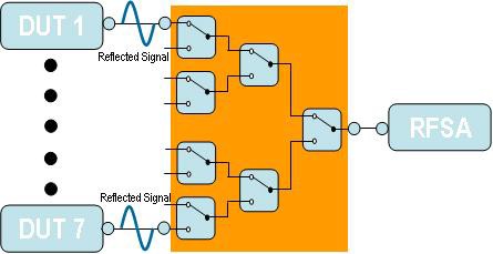
Method 2: Using a module with inherent 8x1 topology
Figure 7. Using an inherent 8x1 multiplexer to route signals from all seven DUTs.
This method uses an inherent 8x1 multiplexer to route signals from all seven DUTs. Because the entire system in this case is contained inside one module, usage of external cables and additional connectors is minimized. Furthermore, signals originating from DUT 1 and DUT 7 will have the exact same path lengths. Hence, insertion loss and signal reflections will be minimal for this set up. Although, using an inherent topology whenever possible, is always recommended, large multiplexers are often hard to find off-the-shelf.
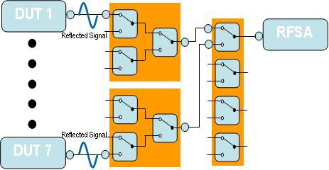
Method 3: Using SPDT relays to build a 7x1 multiplexer
Figure 8. Using SPDT relays to build a 7x1 multiplexer
Although this method of constructing a 7x1 multiplexer is not as efficient as using an inherent 8x1 multiplexer, like in the past example, it is far superior in design to that of the system built in method 1. This is because it uses a Quad SPDT module to route signals from the two 4x1 multiplexers to the RF signal analyzer. By doing so, the switch network allows for equal length paths on each channel of the 7x1 multiplexer. Therefore, although signal reflections and insertion loss will be higher than that of the system in method 2, it will be uniform for all channels.
