Top Measurement Considerations for Modular Source Measure Units (SMUs)
Overview
Learn about how to choose a source measure unit (SMU) based on key features such as IV boundary, precision, source and measure accuracy, measurement speed, source update rate, transient response, and more.
Contents
- IV Boundary
- Precision
- Source and Measure Accuracy
- Measurement Speed
- Source Update Rate
- Transient Response
- Sequencing or Sweeping
- Pulsing
- Channel Density
- Timing and Synchronization
- Software, Analysis Capability, and Customizability
- Connectivity for High-Precision Measurements
- Take the Next Step
IV Boundary
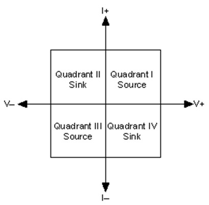
Using a source measure unit (SMU) with the proper IV boundary for your device is critical to the success of your application. The IV boundary is typically illustrated in a quadrant diagram, as in Figure 1, and conveys the voltage and current values the SMU can source or sink. The terms sourcing and sinking describe power flow into and out of a device. Devices that are sourcing power are delivering power into a load, while devices that are sinking power behave like a load, absorbing power that is being driven into them and providing a return path for current.
Figure 1. Quadrant Diagram to Represent Areas of Sourcing and Sinking
In the quadrant diagram above, Quadrants I and III represent sourcing power, while Quadrants II and IV represent sinking power. Devices that are capable of sourcing power in both Quadrant I and III are sometimes referred to as bipolar because they can generate both positive and negative voltages and currents. The term “four-quadrant SMU” is often used to describe bipolar SMUs that source and sink.
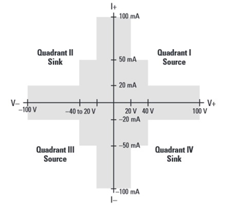
For example, the NI PXI-4132 four-quadrant SMU has a maximum voltage output of 100 V, and maximum current output of 100 mA; however, it cannot simultaneously output 100 V and 100 mA. In this case, the quadrant diagram provides essential detail that gives you the ability to easily determine the maximum voltage and current combinations you can source or sink with the SMU. Simply listing the maximum voltage and current for an SMU with multiple ranges does not give you enough detail to decide if the instrument meets the IV requirements for your device.
Figure 2. NI PXI-4132 IV Boundary
Table 1 summarizes the power capabilities per channel for each NI power supply and SMU device.
| Device | Channel(s) | Quadrant | |||
| I | II | III | IV | ||
| NI PXI-4110 | 0 | 6 W | — | — | — |
| 1 | 20 W | — | — | — | |
| 2 | — | — | 20 W | — | |
| NI PXIe-4112 | 0 and 1 | 60 W | — | — | — |
| NI PXIe-4113 | 0 and 1 | 60 W | — | — | — |
| NI PXI | 0 | 6 W | — | — | — |
| 1 | 40 W | 10 W1 | 40 W | 10 W1 | |
| NI PXI-4132 | 0 | 2 W | 2 W | 2 W | 2 W |
| NI PXI-4138/4139 | 0 | 20 W | 12 W1 | 20 W | 12 W1 |
| NI PXIe-4140/4141 | 0 through 3 | 1 W | 1 W | 1 W | 1 W |
| NI PXIe-4142/4143 | 0 through 3 | 3.6 W | 3.6 W1 | 3.6 W | 3.6 W1 |
| NI PXIe-4144/4145 | 0 through 3 | 3 W | 3 W1 | 3 W | 3 W1 |
| NI PXIe-4154 | 0 | 18 W1 | — | — | 18 W |
| 1 | 12 W1 | — | — | 0.8 W1 | |
| 1See your device specifications for detailed IV boundaries. | |||||
Table 1. Summary of the Power Capabilities per Channel Within the NI Instrument Portfolio
Precision
Measurement resolution of a power supply or SMU is the smallest change in the voltage or current measurement that can be detected by hardware. Output resolution of a power supply or SMU output channel is the smallest possible change that can be made to the output voltage or current level. These measurements are usually specified in absolute units, like nV or pA. Resolution is often limited by the analog-to-digital converter (ADC) used for the measurement, but high-precision SMUs are typically limited by other factors such as noise.
Sensitivity is the smallest unit of a given parameter that can be meaningfully detected with an instrument under specified conditions. This unit is generally equal to the measurement resolution in the smallest range of a power supply or SMU.
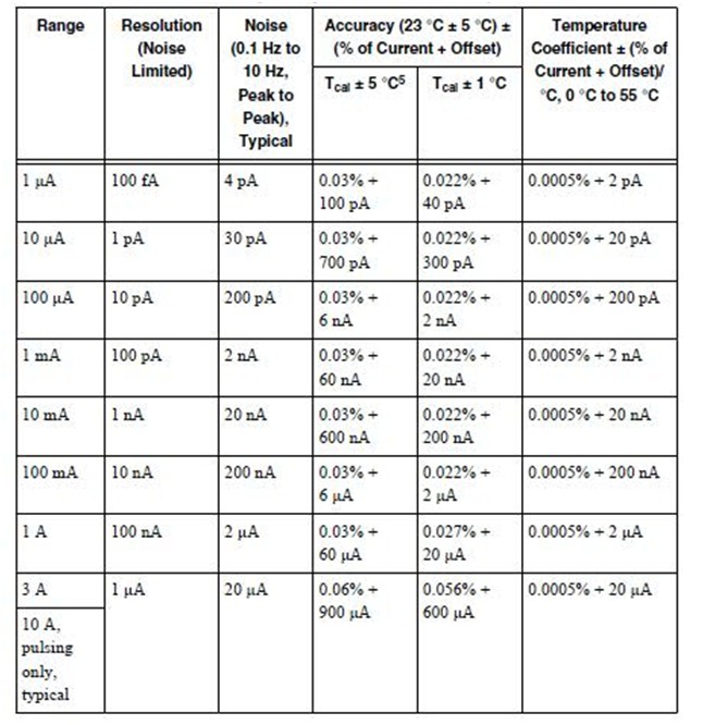
In general, you should use the smallest possible range of the SMU to achieve the best precision. This information is found in the specification manual for the instrument. The following is an example of the table that is provided:
Table 2. NI PXIe-4139 Current Programming and Measurement Accuracy/Resolution
Source and Measure Accuracy
A measurement or output level on a power supply or SMU can differ from the actual or requested value. Accuracy represents the uncertainty of a given measurement or output level and can be defined in terms of the deviation from an ideal transfer function, as follows:
y = mx + b
where m is the ideal gain of the system
x is the input to the system
b is the offset of the system
y is the output from the system
Applying this example to a power supply or SMU signal measurement, y is the reading obtained from the device with x as the input, and b is an offset error that you may be able to null before the measurement is performed. If m is 1 and b is 0, the output measurement is equal to the input. If m is 1.0001, the error from the ideal is 0.01 percent.
Most high-resolution, high-accuracy power supplies and SMUs describe accuracy as a combination of an offset error and a gain error. These two error terms are added to determine the total accuracy specification for a given measurement. NI power supplies and SMUs typically specify offset errors with absolute units (for example, mV or μA), while gain errors are specified as a percentage of the reading or the requested value.
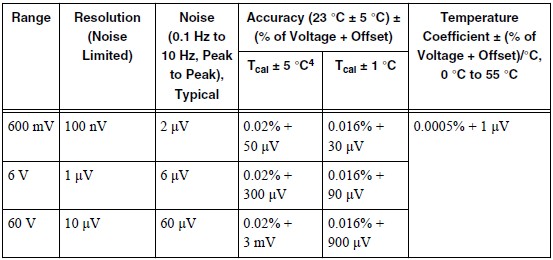
SMUs typically have accuracies for both sourcing and measuring that are at or below 0.1 percent of the output to which they are set. For each NI SMU instrument, you can find this information within the specifications manual.
Table 3. Voltage Programming and Measurement Accuracy/Resolution for the NI PXIe-4139
Measurement Speed
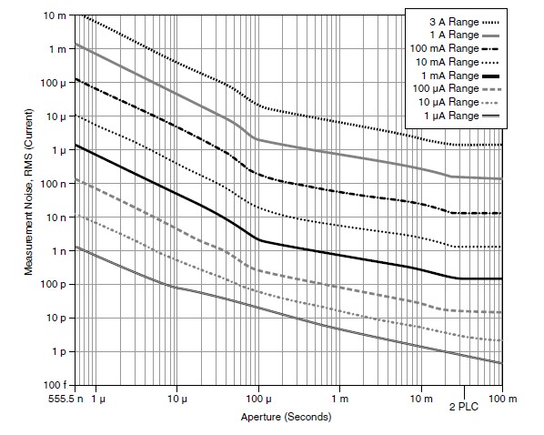
The measurement acquisition window, or aperture time, has a direct impact on the speed and precision of your measurement. Specific SMUs allow you to vary the aperture time of the instrument, giving you the flexibility to extend the acquisition window for high-precision measurements, or decrease the window for high-speed acquisitions. Extending the measurement aperture gives the instrument more time to sample and average, reducing the noise of the measurement and increasing the resolution. The figure below plots the measurement noise as a function of aperture time, at various current ranges.
Figure 3. Example of Noise as a Function of Measurement Aperture
To achieve high-precision measurements, you should use an aperture time that gives you the proper resolution for your measurement, but still minimizes the overall test time. Conversely, you should use short aperture times for lower precision measurements or to digitize signals such as line or load transients. For example, the NI PXIe-4139 can sample up to 1.8 MS/s, giving you the ability to examine the detailed transient characteristics of the SMU output. Depending on your current range, you can achieve this speed with anywhere from 1 nA of noise to 10 mA of noise.
Source Update Rate
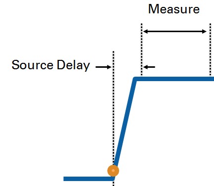
The update rate of the SMU determines how quickly you can modify the output voltage or current of the SMU. For example, an SMU with a 100 kS/s update rate can source a new point every 10 us. SMUs with fast update rates can execute lengthy IV sweeps much faster than traditional SMUs. Additionally, SMUs with fast update rates give you the ability to source nontraditional sequences such as a sine wave.
Figure 4. Control the update rate of an SMU by varying the source delay, or the time between the start of a voltage step and when the measurement starts.
Transient Response
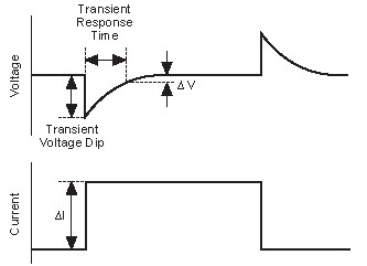
Transient response describes how a supply responds to a sudden change in voltage or current, either generated by an external event such as a change in load, or an internal event such as outputting a voltage step.
External Change in Load
An external change in load current can cause the voltage to change drastically, and temporarily dip below the desired voltage output. The transient response specifies how long it takes before the supply voltage recovers to within a certain voltage (ΔV) when a specific change in load (ΔI) occurs. A fast transient response is critical for powering mobile devices. Large, instantaneous changes to the load current drawn by the device under test (DUT) result in an output voltage dip as the control circuitry of a power supply acts to restore the output voltage to its original value. On typical programmable power supplies, this can often take hundreds of microseconds. Conversely, the 20 µs transient response of the NI PXIe-4154 (available when set to “fast” mode) allows the simulator to quickly respond to changes in load current during tests. This short recovery time is optimal for many wireless communications devices that implement pulsed communications protocols.
Figure 5. Demonstrates How Transient Behavior Is Typically Specified
Changing the SMU Output
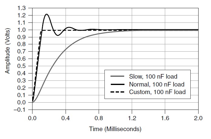
When changing the output of the SMU, the transient settings of the instrument define how fast the output rises and settles at the desired output. An ideal transient response would have a fast rise time with no overshoot or oscillations. There is a trade-off between transient response and the stability of the supply under a wide variety of loads. To achieve the fastest transient response, a device should have a high gain-bandwidth (GBW) product, but the higher GBW is, the more likely it is that the device will become unstable with certain loads. Thus, most devices compromise performance to achieve stability under a broad range of conditions. Other devices allow a small degree of customization to enable optimization of performance under different circumstances. For example, many traditional SMUs offer a “High Capacitance” mode for using the SMU with devices with up to 50 uF of capacitance.
Certain NI SMUs are equipped with a digital control loop technology called NI SourceAdapt, which gives you the ability to custom tune the transient response of the SMU to achieve the optimal response to any given load. This gives you minimal settling times, which leads to shorter wait times and faster test times, and it eliminates overshoots to protect the DUT and oscillations to ensure system stability. Because tuning the SMU response is done programmatically, an SMU configured for a high-speed test can be easily reconfigured for a high-stability test—maximizing the return on investment of the test equipment and achieving better results.
Figure 6. The NI PXIe-4139 features configurable transient response settings for flexible load compensation of the output control loop.
You can see which NI PXI Source Measure Units support SourceAdapt technology, by visiting the NI online catalog and filtering by SourceAdapt.
Sequencing or Sweeping
SMUs typically operate in one of two output modes: single point or sequenced. In single-point mode, the SMU output is limited to one value, however, for sequenced mode, the SMU steps through a series of output values and measures the IV data at each point.
Single-Point Source Mode
Single-point mode is traditionally used for capturing IV data at a single value, such as testing the forward voltage on a diode, or for using the SMU to supply power to your DUT, such as powering an IC with a constant voltage. Some use-cases for single-point mode include developing software-timed sequences where you can loop through a series of single-point SMU outputs in software. Software-timed sequencing can be used in place of hardware-timed sequence mode when an SMU doesn’t support changing a specific feature without planning ahead of time.
Sequence Mode
When the SMU operates in sequence mode, it outputs a series of hardware-timed values, which offers advantages such as a faster and more deterministic output (and synchronization benefits with other PXI instruments). This typically involves the SMU sourcing a DC voltage or current, measuring the voltage and current, and then moving to the next point in the sequence. Depending on the SMU features, you can vary properties such as output level, current or voltage limit, aperture time, and transient response at each step in the sequence. For storing large sequences, SMUs either have dedicated onboard memory, or support low-latency streaming from the host to the SMU. For example, the NI PXIe-4138 and NI PXIe-4139 transfer data from the host PC to the SMU through a high-bandwidth, low-latency PCI Express connection, and allow you to transparently output sequences with millions of setpoints and attributes.
Sequencing is commonly used for applications such as IV characterization or burn-in testing, and is often essential for applications that require tight synchronization with other instruments such as testing RFICs.
Pulsing
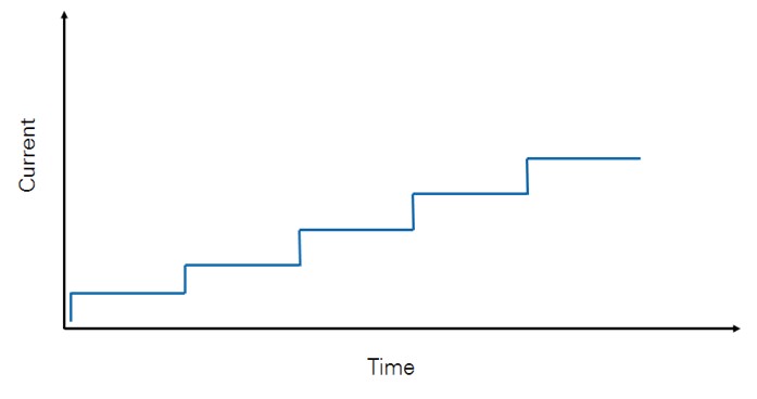
Most semiconductor test applications with SMUs involve some form of source and measure action. When used in sequence mode, this typically involves the SMU sourcing a DC voltage or current, measuring the voltage and current, and then moving to the next point in the sequence. A basic DC sweep incrementally increases the output until the sequence is completed, as in the chart below, which shows a five-step sequence of current values.
Figure 7. Example of a Five-Step Sequence During a Basic DC Sweep
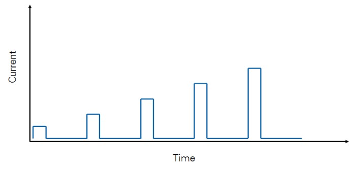
Certain applications, especially high-power applications, can cause incorrect behavior or complicate test setup if you try and sweep through a sequence without turning off the SMU output. For these applications, a pulsed output of the SMU is preferred because it gives you the ability to still source and measure at various setpoints, while minimizing the heat dissipation through the DUT. A pulsed sweep and a DC sweep are similar in that you likely output a setpoint, wait for it to settle, and take a measurement. The main difference with pulse testing is that the source returns to a bias level after a short pulse duration. In most cases, bias level is set to turn off the DUT (for example, 0V or 0A).
Figure 8. A pulsed output allows the source to return to a bias level before moving to the next setpoint.
Under ideal conditions, the pulse sequence and DC sequence in the above two graphs return the same IV data. However, as previously mentioned, the DC sequence dissipates more heat through the DUT, which can cause abnormal behavior and yield poor test results. This is why pulse testing is preferred for these types of applications. When testing in pulse mode, the pulse width should be long enough for your device to reach a full on state to take settled measurements, but short enough to minimize self-heating of the DUT. The importance of a fast, clean SMU response is magnified when pulsing because the SMU is always starting from the pulse bias level instead of gradually increasing the output in small, incremental steps.
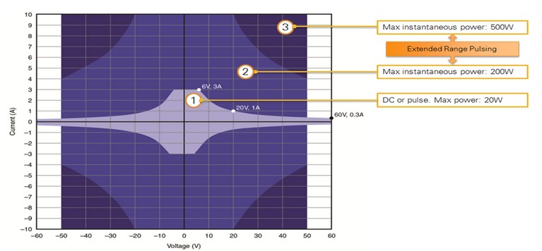
Specific SMUs allow you to generate pulses outside of the traditional DC power boundary to address applications that require higher current. For example, the NI PXIe-4139 can pulse up to 10 A at 50 V for delivering up to 500 W of instantaneous power. Depending on the load and SourceAdapt control settings, pulse widths can be as short as 50 μs. These short pulse widths not only improve test execution time, but also minimize heat dissipation through the DUT, allowing test engineers to perform tests that otherwise might require heat sinks or other thermal control mechanisms.
Figure 9. NI PXIe-4139 IV Boundary
Channel Density
One of the primary advantages of modular SMUs is the compact size. Traditional SMUs have dedicated displays, processors, power supplies, fans, knobs, and other redundant components that complicate the process of building high-channel-count systems. Because modular SMUs use shared components within a chassis and controller, it removes these redundant components resulting in a smaller footprint than traditional instruments. This gives you the ability to decrease the size and power consumption of your test system.
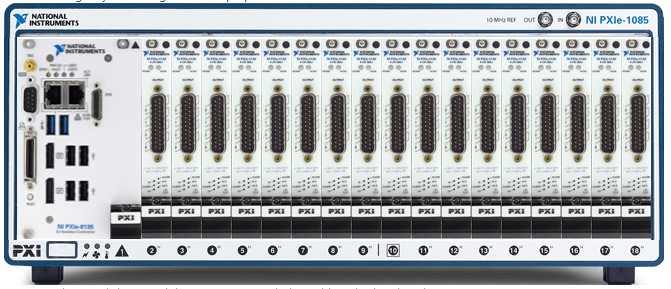
The number of channels required for an application can vary and evolve over time. Many applications require more than the one or two channels on traditional box SMUs. This is especially true for parallel IV test systems in the semiconductor industry, where you need a high number of SMU channels in a compact space. Using NI modular SMUs, you can combine multiple instruments together in a single PXI chassis to create high-channel-count solutions with up to 68 SMU channels in a 19 in., 4U rack space, compared with four to eight channels available with traditional SMUs. The compact size and modularity of the PXI platform also gives you the ability to combine SMUs with other PXI-based instruments such as oscilloscopes, switches, and RF instrumentation to create high-performance mixed-signal test systems.
Figure 10.Use high-density NI SMUs to create systems with up to 68 SMU channels in a single 4U rack size.
Timing and Synchronization
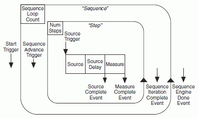
A trigger is a signal to the device to start an operation. An event is a signal from the device that indicates that an operation was completed or a specific state was reached. You can use triggers and events to synchronize operations within a single NI power supply or SMU and operations with other PXI/PXI Express devices. Many applications involve multiple types of instruments such as digitizers, signal generators, digital waveform analyzers, digital waveform generators, and switches. For those applications, the inherent timing and synchronization capability of PXI and NI modular instruments gives you the ability to synchronize all these types of instruments without the need for external cabling.
Using this trigger capability, choose from the following types of triggers:
- Start: The source unit and measure unit do not perform any operations until this trigger is received.
- Source: The device waits for this trigger before the source unit modifies the source configuration.
- Measure: The measure unit takes a measurement when it receives this trigger. While the measure unit is taking a measurement, this trigger is ignored.
- Sequence Advance: The source unit waits for this trigger after an iteration of the sequence completes, just before the next iteration starts.
- Pulse: The source unit waits for this trigger before transitioning from the Pulse Bias to the Pulse Level.
An example of where the PXI platform is optimized for triggering is on the NI PXIe-4138/4139 modules. The modules use the PXI chassis backplane to send and receive triggers and events, which simplifies programming and system wiring. The modules are also hardware-timed and have a high-speed sequencing engine to synchronize handshaking between multiple SMUs.
Figure 11. Sequence Engine Diagram for Triggering and Synchronization
The NI PXIe-4138 and NI PXIe-4139 modules also take advantage of the high-bandwidth and low-latency features of PXI, and support direct DMA streaming between the host PC and SMU. This gives you the ability to transparently stream large waveforms and measurement data at the full update rate (100 kS/s) and sampling rate (1.8 MS/s) of the instrument, removing the bandwidth and latency bottlenecks associated with traditional instrument buses.
Software, Analysis Capability, and Customizability
Determining software and analysis capabilities is very important when choosing a modular SMU for your application, and this factor may help you choose between the two instruments.
Stand-alone SMUs often use basic register-level commands with a vendor-defined functionality while modular SMUs are user-defined and flexible in the applications they can solve. A boxed SMU provides many of the standard functions that are common to the needs of many engineers. As you can imagine, these standard functions do not solve every application, especially for automated test applications. If you need to define the measurements your oscilloscope makes, you might select a modular SMU, which takes advantage of the PC architecture while letting you customize an application to your requirements, instead of the fixed functionality of a stand-alone SMU.
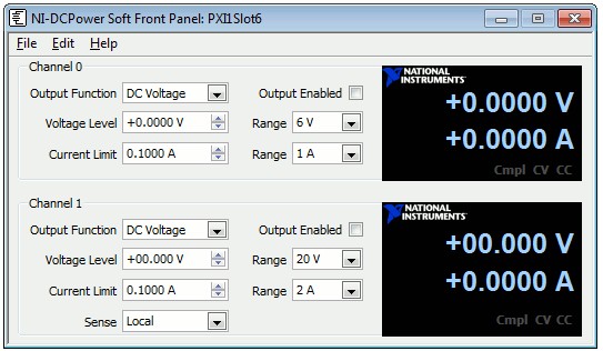
NI SMUs are all programmed using the free NI-DCPower driver software. NI-DCPower, an IVI-compliant instrument driver, is included with your NI power supply or SMU and communicates with all NI programmable power supplies and SMUs. NI-DCPower features a set of operations and properties that exercise the functionality of the power supply or SMU and includes an interactive soft front panel.
Figure 12. Use the soft front panel to quickly make measurements with a modular SMU.
Beyond the soft front panel, use the NI-DCPower driver software to program the modular SMU for both common and custom measurements in a broad range of applications using NI LabVIEW, NI LabWindows™/CVI, Visual Basic, and .NET. The driver also supports express configuration-based functions within LabVIEW.

Connectivity for High-Precision Measurements
Measurements taken using remote sense, sometimes referred to as 4-wire sense, require 4-wire connections to the DUT (and 4-wire switches if a switching system is used to expand the channel count). Using remote sense enables more accurate voltage output and measurements when the output lead voltage drop is significant. When using remote sense in the DC current output function, the voltage limit is measured at the end of the sense leads instead of at the output terminals. Using remote sense results in a voltage at the DUT terminals that is more accurate than what can be achieved using local sense. Ideally, the sense leads should be connected as close to the DUT terminals as possible.
Another aspect to consider is guarding. Guarding is a technique used to remove the effects of leakage currents and parasitic capacitances between HI and LO. Guard terminals are driven by a unity gain buffer that follows the voltage of the HI terminal. In a typical test system where guarding is used, the Guard is connected between the HI and LO terminals. By making this connection, there is effectively a 0 V drop between HI and Guard, so no leakage current flows from HI. Some leakage current might still flow from the Guard output to LO, but, because the current is being supplied by a unity gain buffer instead of HI, it does not affect the output or measurement of the SMU.
As an example, a measurement circuit on the NI PXIe-4138/4139 can simultaneously read the voltage and current values present at the output terminals (local sense) or sense terminals (remote sense). These measurements are performed by two integrating ADCs that are synchronized at all times.
Additionally, as seen in Figure 10, the NI PXIe-4138/4139 features Guard and Sense terminals on the output connector. You can use Guard terminals to implement guarding techniques in cabling and test fixtures. You can use Sense terminals when remote sense is enabled to compensate for current-resistance loss drops in cables and switches.
Figure 14. NI PXIe-4138/4139 features Guard and Sense terminals on the output connector.
Take the Next Step
Modular SMUs can perform equal or better measurements compared to a traditional instrument while offering a platform to support modern technology with measurement and channel capability to meet changing needs. However, the considerations discussed above are important when purchasing either instrument. Thinking ahead about application requirements, cost constraints, performance, and future expandability can help you choose the instrument that best meets all your needs.
- Explore the complete portfolio of SMU instruments
- Get tips and tricks to make the switch to a modular SMU
- Get started with an SMU today with the NI PXI SMU Bundle
The mark LabWindows is used under a license from Microsoft Corporation. Windows is a registered trademark of Microsoft Corporation in the United States and other countries.
