The Controller for FlexRIO: A Deep Dive on Deployable Instrumentation
Overview
The Controller for FlexRIO is a commercial off-the-shelf (COTS) solution designed for applications that require high-performance I/O and real-time signal processing in a compact, stand-alone form factor. The combination of modular I/O, a LabVIEW-programmable FPGA, and an onboard processor gives engineers the ability to fully reconfigure the hardware for specific applications, which sets the Controller for FlexRIO apart from most COTS instrumentation. The controller also shares the same adapter modules, FPGAs, and software experience as FlexRIO on PXI, which makes it an ideal deployment target for solutions developed on the PXI platform. Although it has much in common with FlexRIO in PXI, it is aimed at embedded applications where smaller, lighter, lower power solutions are preferred.
Contents
- Internal Architecture
- FlexRIO Adapter Module Interface
- FPGA
- High-Speed Serial
- Clocking
- Processor
- Connectivity
- Physical Packaging
- Summary
- Next Steps
Figure 1: The Controller for FlexRIO is a stand-alone acquisition and signal processing device with high performance I/O and a large Kintex-7 FPGA.
Internal Architecture
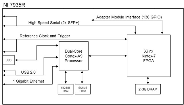
The Controller for FlexRIO is built around a large Kintex-7 FPGA that is connected to a modular I/O interface, a processor, and 2 GB DDR3 DRAM. With over 400,000 logic slices, 1,540 digital signal processing (DSP) slices, and 28 Mb of BRAM, a substantial amount of signal processing can be implemented on the FPGA. The dual-core ARM processor provides network and USB connectivity for interfacing with other devices as well as onboard storage for parameter and data logging.
The combination of a large FPGA and a low-power processor is particularly valuable when most of the algorithms can be implemented on the FPGA, which leaves the dual-core ARM processor for power-on configuration and monitoring of the system. This architecture puts the intelligence closer to the edge, where a high-performance FPGA can be used to turn high-speed data into meaningful information.
Figure 2: With a large Kintex-7 FPGA, the Controller for FlexRIO is ideally suited for applications where signal processing algorithms need to run in real time.
If high-bandwidth data needs to be aggregated at a central location, the NI 7932R and NI 7935R models also feature two high-speed serial ports for data streaming directly from the FPGA using 10 Gigabit Ethernet UDP, Xilinx Aurora, or custom protocols.
FlexRIO Adapter Module Interface
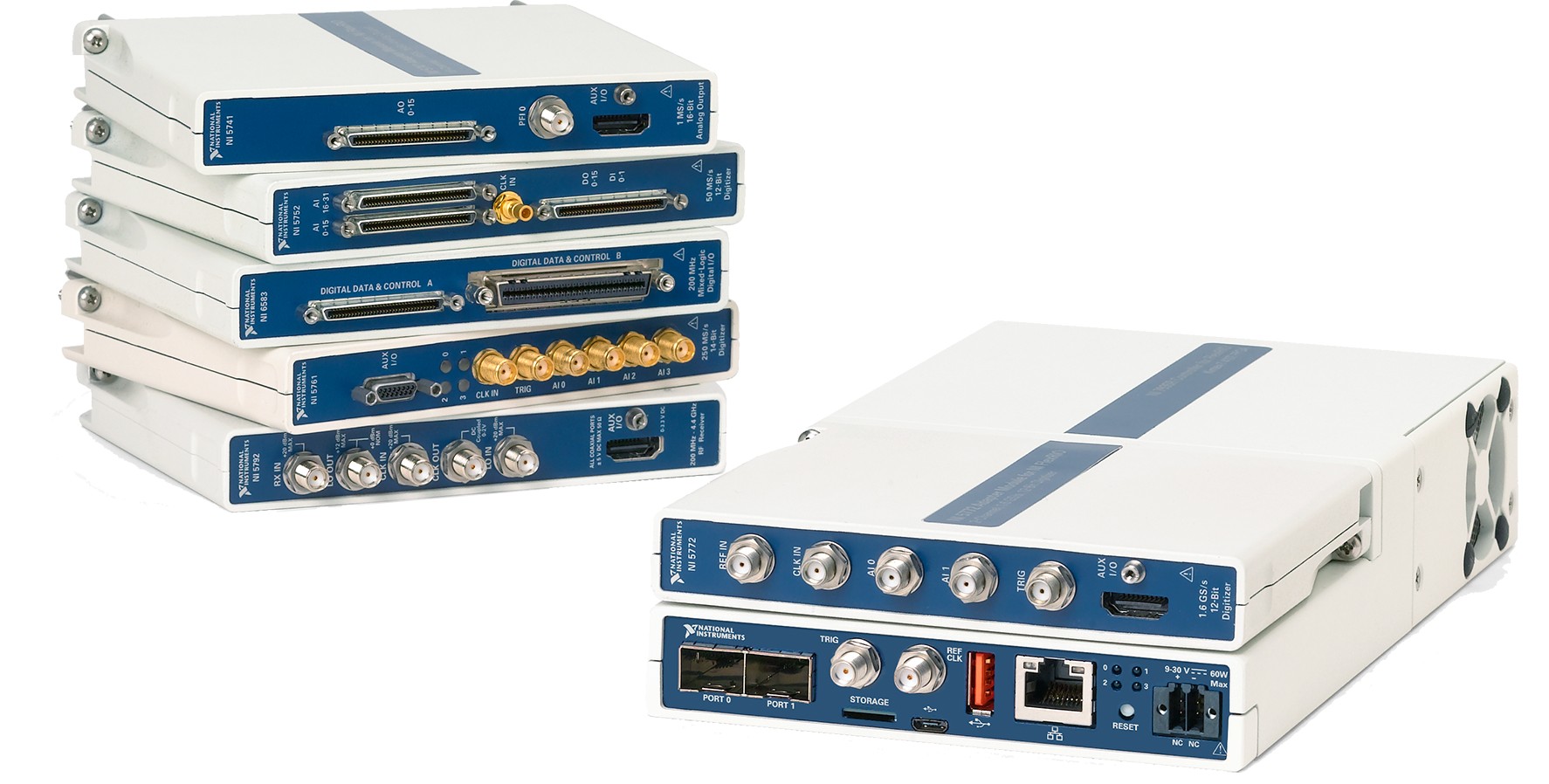
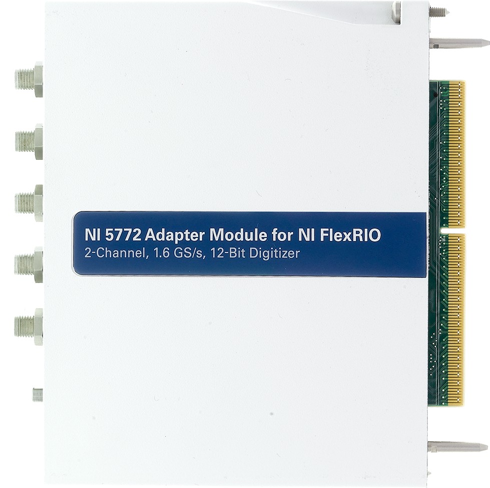
Figure 3: The NI 5772 is a 2-channel high-speed digitizer adapter module commonly used in both time domain and frequency domain measurements.
Learn more about the FlexRIO Module Development Kit
FPGA
Users program the FPGA using LabVIEW system design software with the LabVIEW FPGA Module, enabling both LabVIEW-based algorithm capture and VHDL/Verilog integration. Existing LabVIEW libraries can be used to accelerate development with data movement infrastructure, advanced signal processing functions like an ultra-wideband fast Fourier transform (FFT) and parallel resampling algorithms, and managed DMA streaming to host. Designs can be simulated in LabVIEW before compiling locally or through the NI Compile Cloud Service. After the FPGA bitfile is compiled using LabVIEW FPGA and Xilinx Vivado, bitfiles are deployed through LabVIEW on the development machine; by real-time applications, built with LabVIEW or C/C++, running on the controller; or from the device’s flash on power-up. In many FlexRIO designs, logic is clocked at hundreds of megahertz, where it can be more difficult to meet timing constraints. NI recommends that newer LabVIEW FPGA developers start by reviewing the High-performance LabVIEW FPGA Developers Guide for best practices on both timing and resource optimization.
Figure 4: LabVIEW simplifies FPGA programming by providing an integrated, graphical development environment for design, simulation, debugging, and deployment.
Engineers can choose between two FPGA options: a Xilinx Kintex-7 K325T and a larger K410T. For initial development, using the largest FPGA available has significant advantages. Not only does it give the flexibility to add features during development, but it also provides the ability to compile the same code on a larger FPGA, which generally reduces compile times during design, making faster iteration possible. With NI-provided I/O interfaces, LabVIEW FPGA code written for one hardware target can be quickly ported to other NI hardware, even hardware with different FPGAs and I/O capabilities.
FPGA | Slices | LUTs | Flip Flops | DSP Slices | Block RAM (kb) | Onboard DRAM |
Kintex-7 K410T | 63,550 | 254,200 | 445,200 | 1,540 | 28,620 | 2 GB |
Kintex-7 K325T | 50,950 | 203,800 | 407,600 | 840 | 16,020 | 2 GB |
Figure 5: The Controller for FlexRIO features two different Xilinx FPGAs so that users can choose the right part for the application. NI recommends using the largest FPGA for initial development before attempting to optimize the design for deployment.
DRAM is a resource that adds substantial value in multistage signal processing algorithms and data buffering across nondeterministic buses. To make these types of operations possible, all three variants of the Controller for FlexRIO have one 2 GB bank of DDR3 DRAM attached to the FPGA. The DRAM interface has a data width of 512 bits and is efficiently accessed at clock rates up to 166 MHz, which results in a maximum theoretical bandwidth of 10.6 GB/s between the DRAM and the FPGA. Random access reads and writes decrease DRAM throughput, however, NI has benchmarked sequential reads and writes above 9 GB/s. DRAM can be addressed using the LabVIEW Memory Item in LabVIEW FPGA or as a FIFO using the Memory Instrument Design Library (IDL).
Learn how to use DRAM effectively.
High-Speed Serial
For applications that require high-bandwidth data streaming after signals have been acquired and processed, the NI 7932R and NI 7935R are equipped with two high-speed serial transceivers, each can stream data at up to 10.3125 Gb/s. This technology relies on Xilinx GTX multi-gigabit transceivers (MGTs) that are routed from the FPGA to two SFP+ connectors on the front panel. NI provides LabVIEW FPGA sample projects for 10 Gigabit Ethernet UDP and Xilinx Aurora protocols. Users experienced with VHDL can implement others like Serial RapidIO or custom protocols.
Examples of data streaming configurations that use these high-speed serial ports include sharing data between multiple controllers using Xilinx Aurora, streaming data back to PXI using Aurora or 10 Gigabit Ethernet, and streaming data to a desktop PC, data recorder, Network Area Storage (NAS), or server using 10 Gigabit Ethernet.
Figure 6: The high-speed serial ports are intended for high-bandwidth data streaming to a number of devices. Communication protocols are defined in LabVIEW FPGA and each transceiver can run at up to 10.3125 Gb/s.
Read more about high-speed serial technology in NI products
Clocking
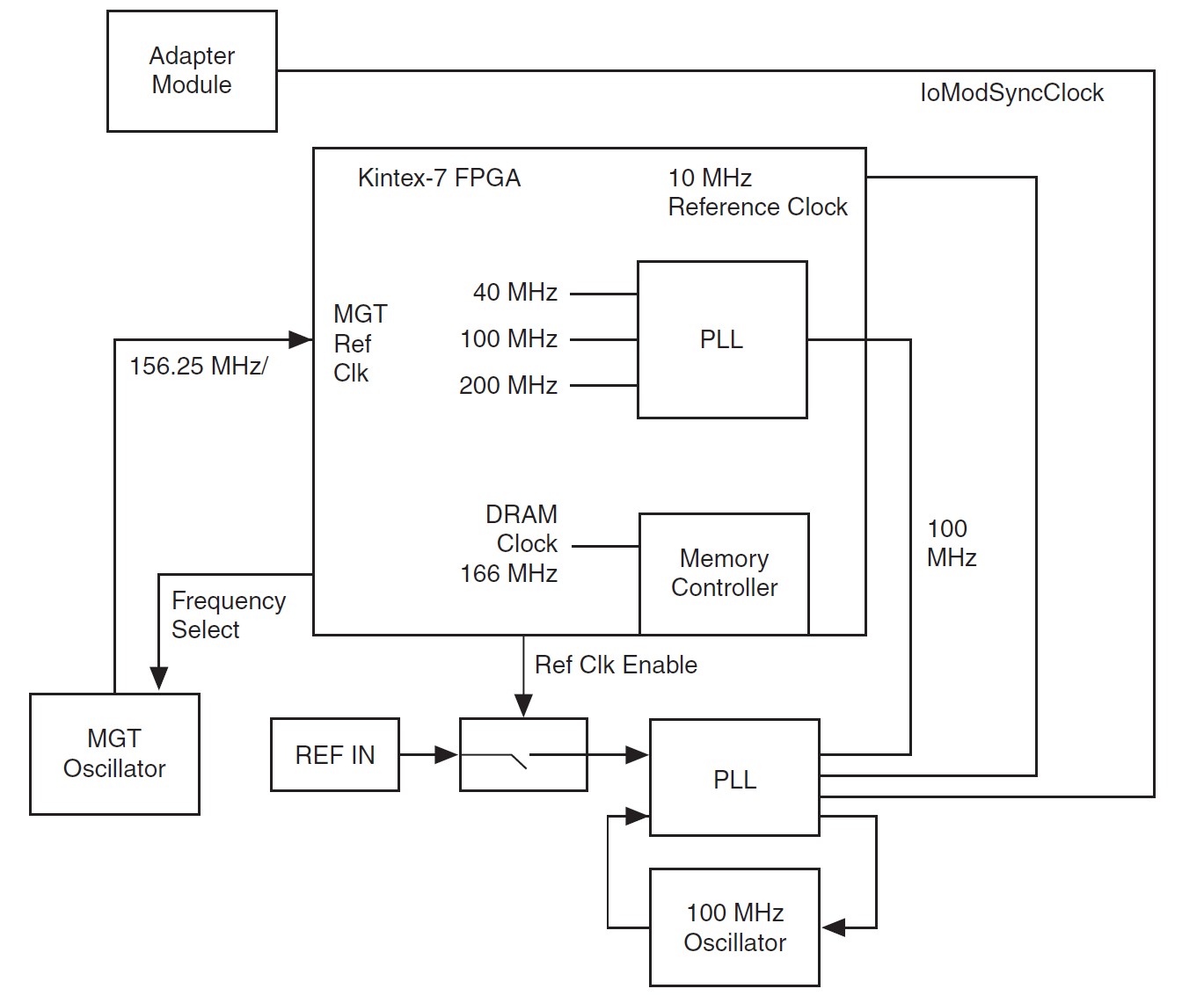
Engineers working with FPGAs and high-speed I/O often spend a good deal of time implementing the proper clocking and synchronization architecture. To simplify this process, the Controller for FlexRIO has a number of clocking options, including an external 10 MHz reference clock input, a bidirectional trigger line, an onboard 100 MHz oscillator, and the ability to phase lock to an external reference. To ensure synchronous data transfer between the I/O module and the FPGA, the I/O module sample clock is shared with the Controller for FlexRIO clocking circuitry. Additional clocks can also be derived on the FPGA.
Figure 7: With the clocking circuitry on the Controller for FlexRIO, users can synchronize multiple devices with subsample accuracy.
For distributed systems and timestamping, a GPS receiver can be connected to supply a 10 MHz clock to the reference clock input and a 1 pulse-per-second input to the trigger SMA. For less stringent synchronization requirements, the NI Linux Real-Time host also supports software-based IEEE 1588. For systems where electrical synchronization is possible, a 10 MHz source like the Ettus Octoclock can be used to provide a shared reference clock. In the case where multiple units are co-located, it is worth considering the advanced clocking and synchronization features of the PXI platform.
Processor
The dual-core ARM Cortex-A9 processor adds the flexibility and connectivity necessary to deploy the Controller for FlexRIO in the field. It can be used to provide data to a network, adjust configuration parameters, log data and messages, or even update the software and FPGA firmware running on the device. The processor runs the NI Linux Real-Time OS, which offers increased determinism and reliability, along with the standard benefits of the Linux kernel. The real-time OS (RTOS) is programmable through LabVIEW with the LabVIEW Real-Time Module and also supports C/C++ development using your preferred integrated development environment (IDE). Programming and building applications from LabVIEW gives developers access to prebuilt libraries for network communication and file I/O, which greatly simplifies development.
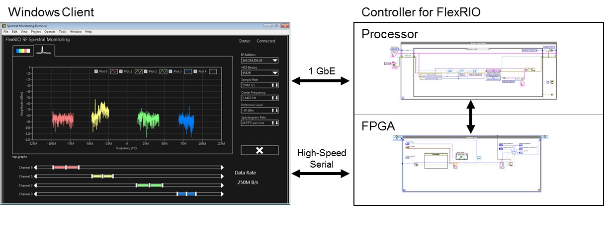
For users familiar with FlexRIO, the primary difference when moving from FlexRIO on PXI to the Controller for FlexRIO is that a network communication layer is added between the FPGA and a traditional Windows client. Instead of targeting the FPGA directly from Windows, code developed for NI Linux Real-Time targets the FPGA and the user is responsible for programming any network communication for monitoring or configuration of the system. On the NI 7932R and NI 7935R, users can take advantage of the two high-speed serial ports for data streaming directly from FPGA through 10 Gigabit Ethernet UDP or Xilinx Aurora.
Figure 8: A deployed system often has three application layers: firmware running on the FPGA, LabVIEW or C/C++ code running on the Linux Real-Time host, and a client application for remote configuration, monitoring, or data logging.
The processor also has access to 512 MB of flash storage and 512 MB of RAM of its own, along with a 1 Gigabit Ethernet interface, USB 2.0 device and host interfaces, and a µSD card slot. The primary interface for deployed applications should be 1 Gigabit Ethernet because it supports substantially more bandwidth; however, the USB device port can be used for setup, configuration, and diagnostics.
Connectivity
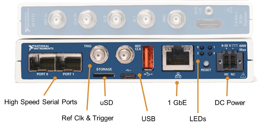
All connectivity is exposed on a single hardware face to make the device easier to integrate into larger systems. Although the I/O is modular, analog adapter modules also provide the FPGA with digital I/O through an auxiliary I/O connector. The controller accepts DC power between 9 volts and 30 volts, which means it can be battery powered for portable systems.
Figure 9: Aside from the connectivity that the FlexRIO adapter modules provide, the Controller for FlexRIO has industry standard interfaces for data streaming, SMA connectors for clocking and synchronization, USB ports for communicating with peripherals, and LEDs for visual status indicator.
All connectors have measures for cable retention with the exception of the two USB ports. The USB host port (color orange) is specially designed for high retention, while the USB device port is intended to be used primarily for diagnostics.
Physical Packaging
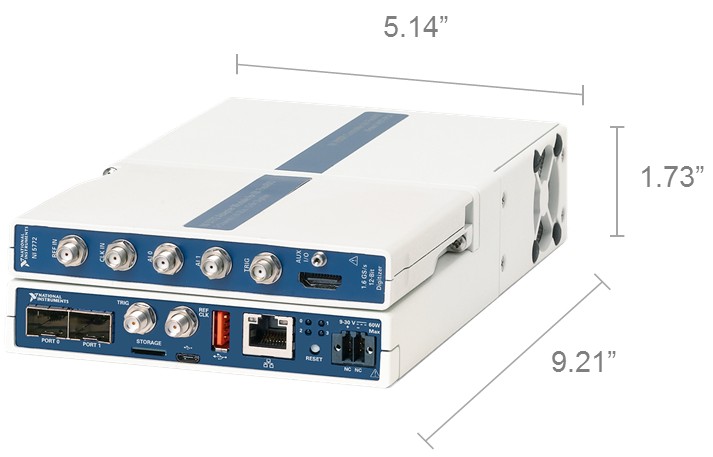
The device’s aluminum enclosure eliminates the need to design custom mechanicals and is intended to make it easy to integrate by providing consistent analog and thermal performance in a variety of scenarios. With the mounting kit, the unit can also be securely panel mounted.
Figure 10: The Controller for FlexRIO is packaged for embedded applications where size, weight, and power are limited.
The packaging also includes several features to ensure long-term reliability and serviceability. First, developers have access to software hooks to monitor FPGA and processor temperatures. In the event that the FPGA or processor temperature exceeds the safe limits, the device automatically shuts down to prevent damage to internal components. Active cooling is provided by a user-serviceable fan that can be monitored in software and adjusted automatically with device temperature. At 40 °C, the mean time between failures (MTBF) of the fan is over seven years.
For scenarios where shock, vibration, temperature, or humidity are a concern, the Controller for FlexRIO is rated similarly to PXI, withstanding 30 g peak half-sine shock, 0.3 grms vibration between 5 Hz and 500 Hz, 0 °C to 55 °C ambient temperatures,and five percent to 95 percent noncondensing humidity.
Summary
The ability to rapidly prototype algorithms that run in real time has been an advantage NI has provided for over a decade with the LabVIEW reconfigurable I/O (RIO) architecture and LabVIEW FPGA. For engineers and scientists prototyping new technologies in areas like radar, spectrum monitoring, communications, industrial machinery, ultrasound, and medical imaging, this platform makes faster prototyping possible with maximum code reuse during productization or deployment.
Next Steps
- Learn more about FlexRIO
- Shop FlexRIO adapter modules
- See the Controller for FlexRIO variants
The registered trademark Linux® is used pursuant to a sublicense from LMI, the exclusive licensee of Linus Torvalds, owner of the mark on a worldwide basis.
