Important Considerations When Migrating to the Digital Pattern Instrument
Overview
The PXI Digital Pattern Instrument brings ATE-class digital to the PXI platform through features and programming that are familiar to semiconductor test engineers. Those features not only come through in the hardware of the instrument, they also appear in the NI-Digital Pattern Driver and Digital Pattern Editor. The digital pattern instrument represents an improved experience to previously existing NI PXI Digital Waveform Instruments, which use the NI-HSDIO device driver. PXI Digital Waveform Instruments do not have this familiar programming method for semiconductor test. For existing customers using PXI Digital Waveform Instruments, particularly the PXIe-6556 or PXIe-6555 (24 channels with per-pin PPMU), there are several considerations when migrating test programs to the PXIe-6570 digital pattern instrument.
Contents
- Migration from the PXIe-6555 and PXIe-6556
- Waveforms to Patterns
- Sample Rates to Time Sets
- NI-HSDIO to NI-Digital
- Programmatic Instrument Configuration to Sheets
- Channel References to Pin Maps
- Instrument-Centric to DUT-Centric Voltage Levels
- Scripting to Opcodes
- Generation and Acquisition to Bursting
- Digital Waveform Editor to Digital Pattern Editor
- Waveform Files to Pattern Files
- Specifications
- Cables and Accessories
- Next Steps
Migration from the PXIe-6555 and PXIe-6556
The PXIe-6555 and PXIe-6556 digital waveform instruments are now on a path to end-of-life. If your application includes one or more of these modules, you may choose to migrate to the PXIe-6570 Digital Pattern Instrument or migrate to another digital waveform instrument depending on the features your application requires. Review the following sections to help you decide which migration path is best for your application.
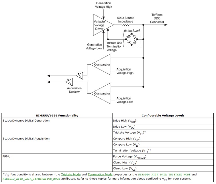
Per-Pin Parametric Measurement Unit (PPMU) and Active Load
The PXIe-6555 and PXIe-6556 digital waveform instruments feature PPMU and active load functionality. Because these are the only digital waveform instruments with this functionality, applications requiring PPMU or active load should greatly consider migration to the PXIe-6570 digital pattern instrument.
Data Rates Beyond 100 Mbit/s
The PXIe-6555 and PXIe-6556 digital waveform instruments acquire and generate data based on a fixed sample clock with a maximum frequency of 200 MHz. The PXIe-6570 digital pattern instrument leverages a more robust timing solution based on vectors rather than samples, allowing flexible and extremely precise configuration of drive and compare edges. The minimum vector period for the PXIe-6570 is 10ns, which allows generation of a 100MHz clock using the return low or return high drive formats available. For data pins, it is more common to use a non-return drive format which results in up to 100Mbps (works well for single data rate interfaces up to 100MHz). For DDR (Dual Data Rate interfaces), data pins update just as frequently as clock pins, and therefore a 100MHz non-return drive format results in 50MHz DDR interfacing. In addition, there is currently one compare strobe in a 10ns period. This means the PXIe-6570 is limited to comparing data at 100Mbps compared to the 200Mbps comparison capabilities of the PXIe-6555/6 hardware. NI has plans to increase data rates of the PXIe-6570 in the near future, if this is a concern for your application, please reach out to your local NI representative. A more detailed explanation of the timing differences between digital waveform and digital pattern instruments can be found in the Samples to Timesets section later in this document.
DUTs with More Than 32 Pins
For an application synchronizing multiple PXIe-6555/6 instruments to interface with a DUT with greater than 32 pins, migration to the PXIe-6570 may require additional calibration steps to achieve cross-instrument pin alignment.
PXI Digital Waveform Instrument Options
The PXIe-6544 and PXIe-6545 are 32-pin, 100 MHz and 200 MHz digital instruments intended for interfacing with numerous standard voltage levels for single-ended interfaces. These instruments are capable of data deskew and data delays on a per-bank basis that enable interfacing with DUTs, protocol testing, and skew adjustments due to cables or other impairments.
The PXIe-6547 and PXIe-6548 are 32-pin, 100 MHz and 200 MHz digital waveform instruments capable of generation high voltage levels between 1.2 V and 3.3V and input protection up to 5 V. These cards also offer per-bank data delays and deskew that enable interfacing with DUTs, protocol testing, and skew adjustments due to cables or other impairments.
The table below compares the PXIe-6555/6 with the PXIe-6570 Digital Pattern Instrument and the PXIe-6544/5/7/8 Digital Waveform Instruments:
| PXIe-6555/6 | PXIe-6570 | PXIe-6544 | PXIe-6545 | PXIe-6547 | PXIe-6548 | |
| Instrument Type | Digital Waveform | Digital Pattern | Digital Waveform | Digital Waveform | ||
| Driver | NI-HSDIO | NI-Digital Pattern | NI-HSDIO | NI-HSDIO | ||
| Number of Bidirectional Channels | 24 | 32 | 32 | 32 | ||
| Logic Levels and Range | -2V to 7V | -2V to 6V | 1.2V, 1.5V, 1.8V, 2.5V, 3.3V | 1.2V – 3.3V | ||
| Programmable | Programmable | Selectable | Programmable | |||
| Advanced Overvoltage Protection | No | Yes | No | No | ||
| Maximum Supported Data Rate | 200 Mbps | 100 Mbps | 100 Mbps | 200 Mbps | 200 Mbps with DDR | 400 Mbps with DDR |
| Supported Data Formats | Non-Return | Non-Return Return to Low Return to High Surround by Complement | Non-Return | Non-Return | ||
| Hardware Compare | Yes | Yes | No | Yes | ||
| Supports PPMU | Yes | Yes | No | No | ||
| Supports Active Load | Yes | Yes | No | No | ||
Waveforms to Patterns
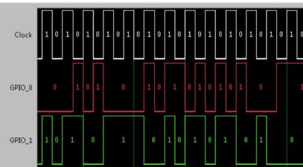
Digital Waveform Instruments, such as the PXIe-6555 or PXIe-6556, rely on a waveform-based paradigm to define the data generated or compared. In a waveform paradigm, output values and expected input values are limited to a fixed sample rate which results in the same sample period used throughout the waveform.
Figure 1. Digital waveform instruments use a waveform data format consisting of evenly spaced samples.
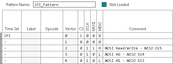
The PXIe-6570 Digital Pattern Instrument moves away from the waveform-based paradigm and into a pattern-based paradigm where input and output values are defined with vectors rather than samples. which have their own timing characteristics on a per-vector basis. This provides the user much more control over the drive and compare values.
Figure 2. Digital pattern instruments burst patterns that can use a number of timing configurations or level configurations that are defined separately from the data.
More information about patterns can be found in the Digital Pattern Help documentation.
Sample Rates to Time Sets
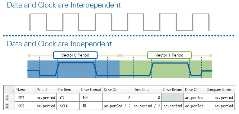
Digital Waveform Instruments use a sample clock edges to define bit transition or compare states. This leads to oversampling the digital data to add additional timing resolution to the waveform, which means larger waveform files with multiple data points per clock period. The cost of time to load memory and manage the size of these files presents some challenges when building an application. Oversampling only provides coarse resolution for edge placement in your waveform, limited by the fastest clock time base you could create with your instrument.
Figure 3. Digital waveform instruments could only assert changes in line value on a pre-defined clock edge. Digital pattern instruments can place data transitions arbitrarily within a vector on a cycle-by-cycle basis.
Digital Pattern Instruments introduce the concept of time sets, which allow flexible, high-resolution timing configuration. Each time set defines the vector period across all pins and allows per-pin configuration of the drive format and drive and compare edges (the PXIe-6570 has an edge placement resolution of 39.0625 ps). Each vector in a pattern consists of a defined time set as well as data values for each pin. The separation of data and timing definitions enables more flexible and modular pattern creation using a fraction of the file size required by digital waveform instruments.
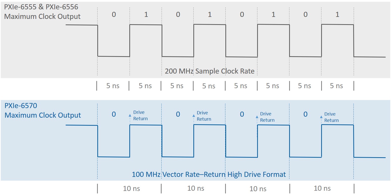
A key specification of the digital pattern instrument is its vector rate. The maximum vector rate of the PXIe-6570 is 100 MHz, which is equivalent to a minimum vector period of 10 ns. This specification is not functionally equivalent to the maximum clock rate defined for digital waveform instruments: a digital waveform instrument is only capable of non-return generation a comparison at the defined sample clock rate, while a digital pattern instrument allows flexible placement of drive and compare edges within a vector period. For instance, a digital waveform instrument with a 200 MHz sample clock rate can change state every 5 ns, which means a data pin could generate a clock signal with maximum 100MHz (5ns low, 5ns high). The digital pattern instrument, however, has return high or return low drive formats that allow two bits to be driven in a single vector period. This allows a PXIe-6570 pin to also generate up to a 100MHz clock signal. This difference is illustrated in Figure 4 which compares the maximum clock generation on a data pin for the PXIe-6555/6 and PXIe-6570.
Figure 4. The PXIe-6555 and PXIe-6556 are capable of generating a 100 MHz clock signal on a data pin to a DUT with a 200 MHz sample rate. The PXIe-6570 is also capable of generating a 100 MHz clock to a DUT with a 100 MHz vector rate due to the flexible definition of drive formats with digital pattern instruments.
Due to this difference in timing behaviors, some digital waveform instruments are capable of generating and acquiring digital data at a higher rate than the PXIe-6570, namely the PXIe-6545, PXIe-6548, PXIe-6555, and PXIe-6556. We have plans to increase data rates for the PXIe-6570, reach out to your local NI representative is this is a requirement for your application.
More information about timing with digital pattern instruments can be found in the Digital Pattern Help document.
NI-HSDIO to NI-Digital
Digital Waveform Instruments use the NI-HSDIO driver for programmatic control of several instrument features. The driver framework consists of a dual session-based architecture, where a user creates a Generation Session and an Acquisition Session per instrument to access the digital I/O on the device. The driver is supported in LabVIEW, C, or a .NET Wrapper.
Figure 5. There are a number of differences between the NI-HSDIO instrument driver and the NI-Digital Pattern Driver, but one of the largest differences is that acquisition and generation required separate tasks when using NI-HSDIO. When using the NI-Digital Pattern Driver, a single pattern can include acquisition and generation operations.
Digital Pattern Instruments use the NI-Digital driver for programmatic control. This driver is not compatible with NI-HSDIO, which means migration will require modification to the user’s code-base to incorporate the new API. There is only one session per instrument in the NI-Digital Pattern Driver, where a user can programmatically burst patterns that contain both drive and compare states. Language support extends to LabVIEW, .NET and C.
Programmatic Instrument Configuration to Sheets
For Digital Waveform Devices, the NI-HSDIO API is used to define and apply session configurations, such as sample rate, data delay, and voltage levels, to the instrument when the code is executed. Because this method of configuration requires code changes for any changes to configured values, users will often use classes or build their own in-house custom file type to pass settings throughout their VI architectures.
Digital Pattern Instruments offer a more modular approach to configuration: instrument configurations are saved in external files called sheets and loaded to the digital pattern instrument. Sheets can be created and edited in the Digital Pattern Editor and include the Timing Sheet, which defines time sets, the Levels Sheet, which defines the drive and compare voltages, and the Specifications Sheet, which contains user-defined variables able to be used within other sheets. These sheets can loaded manually with the Digital Pattern Editor (DPE) or programmatically with the NI-Digital API. This provides an easy way to transfer configuration settings, manage multiple configurations, and also migrate debugging configurations from DPE to your application development environment.
Channel References to Pin Maps
When using Digital Waveform Instruments, channels are defined and configured using the NI-HSDIO API within the code-base. These channels are referenced using an instrument-centric channel number, requiring the user to maintain a knowledge of which instrument channels connect to which DUT pins throughout the application. Additionally, an instrument-centric channel definition requires a code-base change if that instrument is replaced or upgraded at a later time.
Digital Pattern Instruments use a user-configurable Pin Map file to map logical pin names and pin groups to specific instrument channels in their application. The pin map file can expand across multiple instruments and allows the user to work with abstracted, intuitive DUT and system pin names rather than instrument channel numbers. The pin map can be saved and loaded to any number of instruments, and multiple pin map files can be managed to create a configurable programmatic environment that can handle many different types of DUTs with minimal rework of the application code.
Instrument-Centric to DUT-Centric Voltage Levels
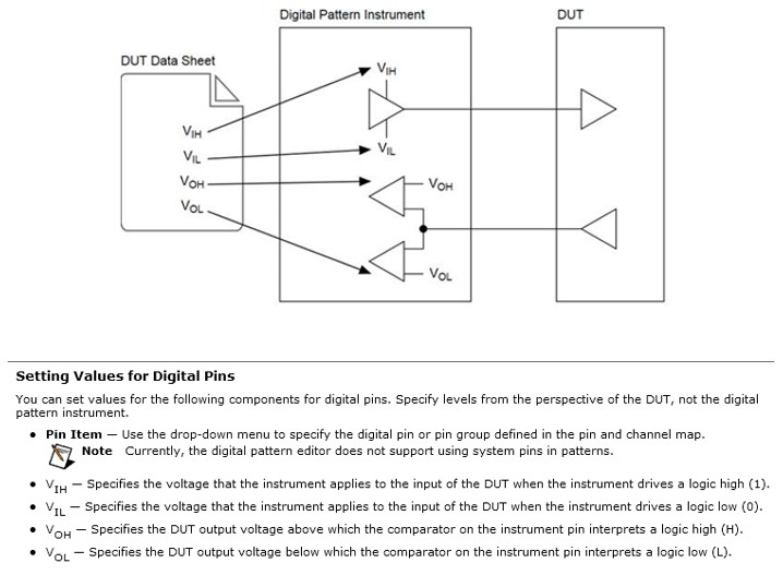
Digital Waveform Instruments use an instrument-centric approach to define voltage levels. For instance, VIH and VIL are defined as the high and low thresholds when comparing a voltage being input to the digital waveform instrument, while VOH and VOL define the voltage output levels driven by the instrument.
Figure 6. The levels used by the channel drivers and comparators of digital waveform instruments consider the instrument as the focus of the test program.
Digital Pattern Instruments shift to a DUT-centric method to define instrument voltage levels. In the NI-Digital Pattern Driver and Digital Pattern Editor, VIH and VIL define the thresholds for the DUT to register high and low values, which the instrument must drive. Similarly, VOH and VOL define the high and low output voltages from the DUT and are used by the digital pattern instrument to properly compare data with expected values. A DUT-centric approach allows users to maintain terminology consistency between the DUT’s data sheet and the instrument configuration. A test engineer can now directly use the VIH/VIL/VOH/VOL values from the DUT data sheet without translating to instrument-centric terminology.
Figure 7. The levels used by the channel drivers and comparators of digital pattern instruments reference the DUT rather than the instrument.
Scripting to Opcodes
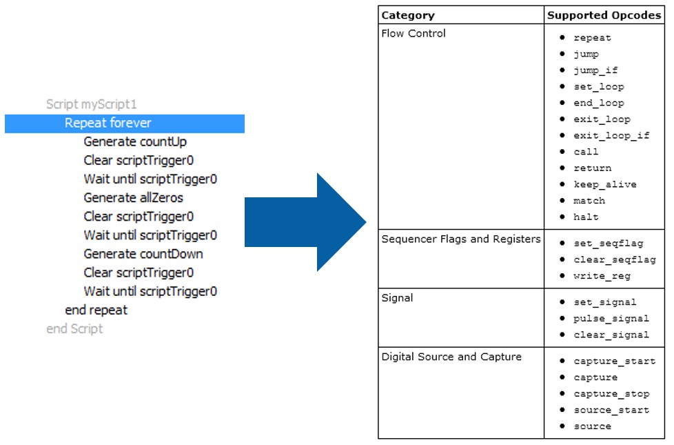
Digital Waveform Instruments perform non-linear, dynamic or repetitive I/O through the use of scripting. The scripting language enables modularity through sequencing of multiple waveforms, memory optimization through cycling of repeatable waveforms, and flexibility through dynamic behavior based on logic and triggers. However, scripting is defined separately from waveforms, which can result in limitations to behavior supported on digital waveform instruments.
Figure 8. Digital waveform instruments use scripting to generate digital waveforms with logical loops. Digital pattern instruments have opcodes that significantly extend logical pattern bursting capabilities.
Digital Pattern Instruments use opcodes rather than scripting for advanced I/O behavior. Opcodes allow a user to perform looping, linking, conditional branching, handshaking (sequencer flags and registers), and more. Furthermore, digital source opcodes replace and extend the abilities of dynamic waveform scripting. Opcodes are configurable on a per vector basis, providing the user with more flexible and full-featured I/O control.
Generation and Acquisition to Bursting
Digital Waveform Instruments perform all digital I/O through two operations: generation and acquisition. Generation sessions output values from the instrument based on a waveform file while acquisition sessions analyze or store digital data received by the instrument. For bidirectional operations, such as a stimulus/response test, both a generation and acquisition session must be configured for the application.
Digital Pattern Instruments are managed through a single session for both input to and output from the instrument. The behavior of the instrument is defined by the pattern data on a per-pin, per-vector basis – the pattern may contain drive values (0, 1, D) or compare values (L, H, M, V, X). Data may be captured at runtime using a capture waveform that a user preconfigures in the driver and pattern file.
Digital Waveform Editor to Digital Pattern Editor
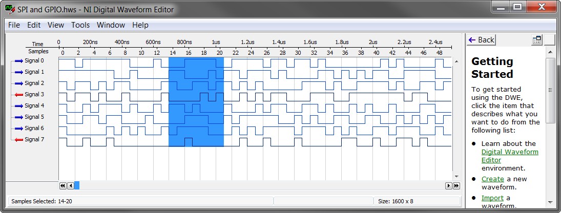
The Digital Waveform Editor (DWE) application allows users to create and modify waveform files with a user interface rather than through text editing or programmatic creation. DWE is scoped to simple waveform editing and does not allow the user to interact with hardware directly. Instead, the user must export the waveform from DWE and load the waveform using the NI-HSDIO API in their development environment.
Figure 9. The Digital Waveform Editor allows a user to build the digital data of a waveform in a graphical environment and export that data to a file format that can be used by the NI-HSDIO driver.
Digital Pattern Instruments come with an all-encompassing application software environment, called the Digital Pattern Editor (DPE). DPE allows users to not only modify pattern data, but perform a variety of code development and debug operations, such as the following:
- Debug patterns using the pin view pane while interacting with the instrument and its features in real time
- Analyze burst pattern results using History RAM (HRAM), Shmoo plots, and Digital Scope features
- Organize files into projects that can be stored and loaded on multiple development machines
- Import or Export pattern files from other projects
- Remote debugging of code that is already running in your ADE to report the status and manually control the instrument at any point in your code
- Create timing, levels, and specifications sheets for instrument configuration
- Create pin maps to logically define pin names connected to physical channels on the instrument
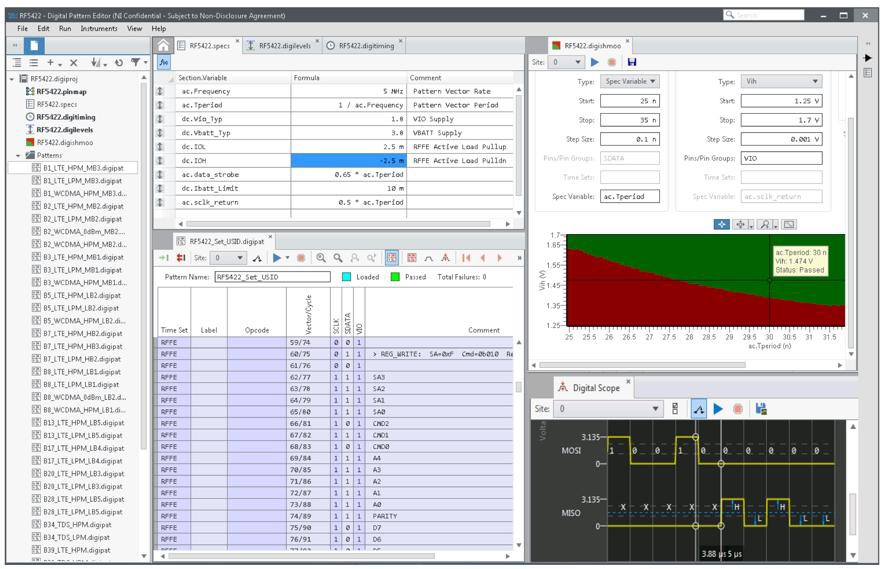
Figure 10. The Digital Pattern Editor is an integrated software environment for developing and editing configuration files like pin maps, specifications and levels, as well as digital pattern data and timing sheets. It also includes debugging and margining tools like a digital scope and Shmoo.
Waveform Files to Pattern Files
Digital Waveform Instruments are able to import and export waveform data using multiple file formats including hierarchical waveform files (.hws), text files (.txt), and binary files (.bin) files. These formats are not consistent and it is often difficult to extract metadata such as timing information.
Digital Pattern Instruments store pattern data in a single compiled digital pattern file (.digipat). is able to be edited directly from the Digital Pattern Editor or loaded to the instrument using the NI-Digital API. DPE can also import or export an additional human-readable format (.digipatsrc), convenient for flexible programmatic pattern creation or migration from other text-based formats.
Industry-common WGL and STIL pattern files could be converted for use with the NI-HSDIO driver using the TD-SCAN tool from TSSI, but the conversion was limited because the PXIe-6555 and 6556 were not designed with a flexible timing format.
Because the NI-Digital driver is able to import text-based .digipatsrc files, third-party converters and EDA tools can be developed to migrate several digital pattern file formats for use with NI digital pattern instruments.
If your application already uses waveform files created using Digital Waveform Editor (.hws, .bin, or .txt), you can use the following tool to convert these files for use with Digital Pattern Editor an the NI-Digital driver:
Specifications
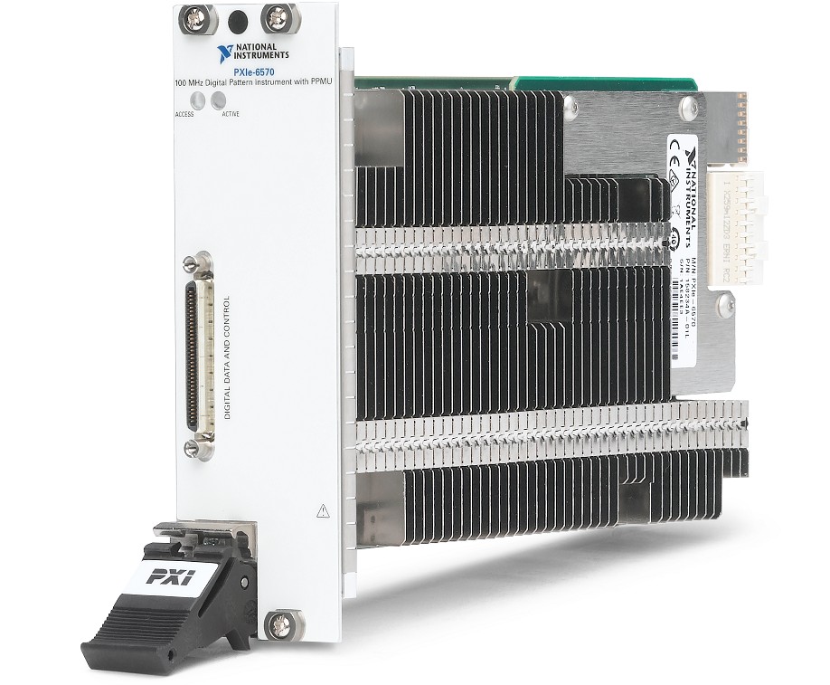
Here is a side by side comparison of key specifications and differences between the PXIe-6556, PXIe-6555, and PXIe-6570:
 |  | |
| Specification | PXIe-6555 and PXIe-6556 | PXIe-6570 |
| Pin Electronics | DCL: -2 to +7 V, 35 mA PPMU: -2 to +7 V, 32 mA Active load: 24 mA | DCL: -2 to +6 V, 32 mA PPMU: -2 to +6 V, 32 mA Active load: 24 mA |
| Channels | 24 channels | 32 channels (up to 256 channels calibrated in STS-Dx) |
| Clock Rate1 | 200 MHz | 100 MHz |
| Data Frequency2 | 100 MHz | 100 MHz (RL, RH, NR) 50 MHz (SBC) |
| Timing | 800 Hz to 200 MHz <0.1 Hz period resolution Fixed time base 5 ns edge placement resolution | 25 kHz to 100 MHz 38 fs vector period resolution 31 timing sets, per cycle adjustment 39.0625 ps edge placement resolution |
| Pattern Formats | Non-Return | Non-Return (NR), Return-to-Low (RL), Return-to-High (RH), Surround by Complement (SBC) |
| Memory Depth3 | Up to 64 Mbits per channel | 128Mvectors / channel |
| PPMU Sense | Local and Remote Sense | Local Sense |
| PFI Lines | 2 PPMU-enabled, 2 high-speed, 2 clocking, 8 high drive strength | None |
1 Clock rate is the maximum clock frequency you may configure on the instrument.
2 Data Frequency is the physical frequency of the data coming out of the channels/pins on the instrument. For the 6556, the maximum data frequency is half the clock rate. For the 6570, depending on the data format, you may burst a 100 MHz digital signal with return-to data formats, while non-return and surround-by-compliment burst digital signals at half the clock rate.
3 Memory depth for the 6556 is in samples, where the memory depth may change based on the configured data width and the purchased memory option of the instrument. Memory depth for the 6570 is in vectors and is always specified at 128 Mvectors for all options and configurations.
Cables and Accessories
Existing cables and accessories for the Digital Waveform Instruments will be electrically compatible with Digital Pattern Instruments. The electrical compatibility allows you to reuse your existing SHC68-C68-D4 Cable, Flying Lead, and connector block accessories for your application. Note: The labels on each accessory may not match up with all pins on your Digital Pattern Instrument.
Pogo Pin Cable Exception: For NI Semiconductor Test Systems (STS) the PXIe-6556 DX pogo pin cables are not interchangeable with the PXIe-6570 DX pogo pin cables. You must use the PXIe-6570 DX cable wtih the PXIe-6570 module.
DUT Interface Board (DIB): You may use the DIB from the PXIe-6556 STS application with your PXIe-6570 if these two conditions are met:
- Only the first 24 channels were used in the PXIe-6556 application
- If PFI Lines were used in the PXIe-6556 application, they must be evaluated.
Examples:- If the PFI line drove a static value and is connected to a 6570 digital channel, the DIB is compatible for that PFI line.
- If the purpose of the PFI line was for receiving a clock or trigger, the DIB would not be compatible on that PFI line.
