Waveform Match Triggering with Software-Defined Instruments
Overview
Software-designed instruments represent a new and revolutionary family that provides out-of-the-box functionality like other modular instruments, but also features a user-programmable FPGA. Users can load new functionality into these instruments, which can either be provided by NI and NI Partners or created by the end user. In this white paper, we explain how you can implement a new kind of trigger functionality for software-designed instruments. Although we use the NI PXIe-5171R reconfigurable oscilloscope in this example, you can also use the trigger functionality on other software-designed instruments such as NI RF analyzers with user-programmable FPGAs.
Contents
- A New Trigger for Oscilloscopes
- The Software Environment
- Trigger Methodology in the Multirecord Acquisition Sample Project
- Creating the Waveform Match Trigger
- Implementation Details
- Multirecord Sample Project With Added Waveform Match Trigger
- Conclusion
A New Trigger for Oscilloscopes
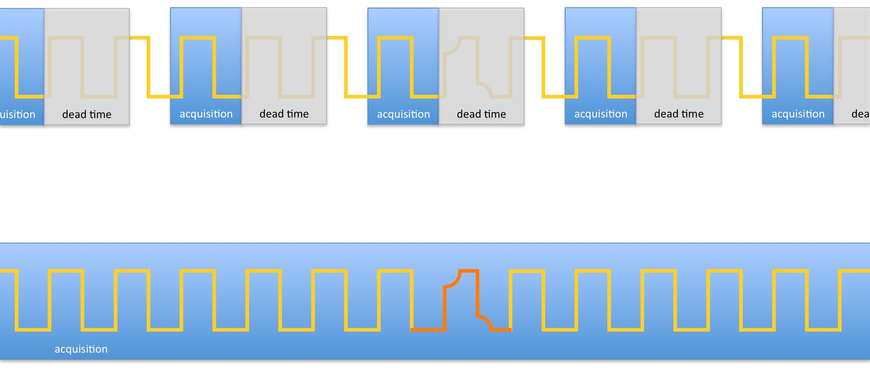
Oscilloscopes provide a wide variety of trigger functions ranging from standard edge detection to identifying specific data content in serial protocols to start an acquisition. However, because of internal rearm times of the oscilloscopes and data processing, the instruments introduce dead time between acquisitions, during which, part of the signal is lost. This dead time can easily be 90 percent or more.
Here, we show you how to design a better trigger that doesn’t have dead time or miss any samples or events, therefore, shortening test times in design or manufacturing and enabling the detection of missing particles in physics research.
Figure 1: Comparison Between Traditional Oscilloscope Dead Time and Reconfigurable Oscilloscope Without Dead Time
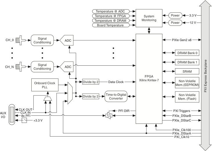
Reconfigurable oscilloscopes such as the NI PXIe-5171R use an FPGA in the data path, behind the analog-to-digital converters (ADCs), which can process every sample of the acquired signal in real time without skipping parts of the signal.
Figure 2: Architecture of the NI PXIe-5171R Reconfigurable Oscilloscope
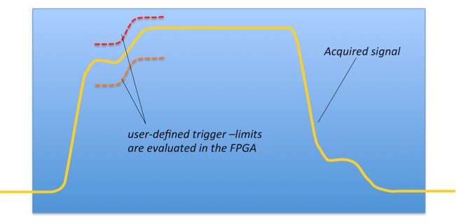
The new trigger we discuss in this example continuously compares the acquired signal to a reference. Whenever the shape of the acquired signal is within the bounds of the user-defined reference, the signal is acquired and sent to the PC for display and further processing.
This trigger is useful for capturing very rare events in electronic design or science experiments where waveform shape matters. We call this a Waveform Match Trigger.
Figure 3: Overview Drawing of How the Waveform Match Trigger Works
The Software Environment
Software-designed instruments are shipped with driver software and instrument design libraries (IDL) for developing custom IP. These IDLs consist of LabVIEW VIs that encapsulate low-level tasks, such as configuring the ADC and applying calibration data as well as corresponding VIs for the host that controls the FPGA code.
Software-designed instruments also include sample projects that provide starting points for custom IP development. For the NI PXIe-5171R reconfigurable oscilloscope, two different sample projects are provided:
- Stream to Host Sample Project—Allows streaming of the acquired samples in finite transmissions or continuously to the host computer for processing or storage on a hard drive
- Multirecord Acquisition Sample Project—Resembles the basic functionality of an oscilloscope with options to set input ranges, sample rates, record sizes, triggers, decimation, and so on; used to implement the new Waveform Match Trigger
Before we dive into the implementation of the trigger itself, here’s an overview on the operation of the Multirecord Acquisition sample project as well as the main components and data types used.
Figure 4: Block Diagram of the Multirecord Acquisition Sample Project
For a detailed explanation of the sample project, refer to the documentation installed with the driver software for the hardware; the documentation of the sample project, which is available from within the project in LabVIEW; and the documentation and context help of the VIs of the IDLs used in the sample project.
Trigger Methodology in the Multirecord Acquisition Sample Project
For the Multirecord Acquisition sample project, the triggering requirements are defined by the Multirecord Acquisition IDL IP. This IDL is installed with the NI PXIe-517xR. You can find documentation for it in the installed help file.
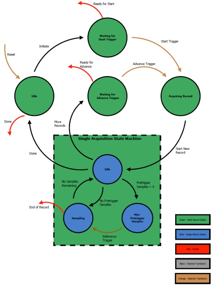
Figure 5: Multirecord Acquisition State Machine
The multirecord acquisition state machine illustrated in Figure 5 shows all the states an acquisition goes through. The light brown arrows indicate external events, or triggers (inputs), that control the flow between the available states. We can manipulate these triggers to make our custom trigger logic. In this context, “external” means external to the Multirecord Acquisition IDL and provided to it through our custom code. Although we can use the digital connector to provide external hardware signals as triggers, we can also configure these triggers to be based from software (code) events. For example, with immediate triggering, the Reference Trigger is always provided a TRUE constant, so that it immediately goes from pre-trigger sampling to post-trigger sampling without delay. This is different from edge triggering, which waits to provide a Reference Trigger until the analog waveform has crossed the configured threshold.
The three triggers referenced in this state chart (orange) are the Start Trigger, the Advance Trigger, and the Reference Trigger. Their associated events are illustrated above in red. Events are output signals from the multirecord acquisition state machine, which can also be used. They are like status updates that let us know which state the acquisition engine is in, and they can help us perform synchronized measurements. For example, by exporting the “Ready for Start” out of the digital I/O port, we could signal to the device under test (DUT) that we are ready to take a measurement. This is just one way these signals could be used for DUT control.
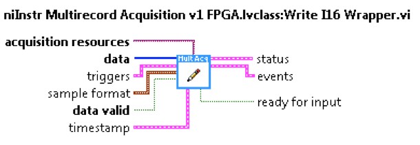
The Multirecord Acquisition Write Wrapper.vi in the FPGA is where the multirecord acquisition state machine is implemented. It is through this VI that we get the events, and where we send the trigger information. This VI maintains the current state of the acquisition and evaluates, based on the trigger and timestamp inputs, the sampling state of the hardware and whether to ignore or save the provided data value into memory, which by default is implemented in DRAM.
Figure 6: Screenshot of Write I16 Wrapper.vi From the LabVIEW Context Help
Default Triggering
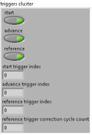
The triggers input, as seen in Figure 6, is a LabVIEW cluster with a set of Booleans indicating the type of trigger, and a set of integers indicating the index the trigger occurred. Because multiple samples are generated per cycle, the trigger index is used to distinguish which sample caused the trigger condition. For the NI PXIe-5171R family, this is either 0 or 1 because the hardware generates two samples per cycle (2 SPC). The Boolean values in the trigger cluster are level-sensitive and evaluated during the states indicated in Figure 5.
Figure 7: Snippet of the Triggers Cluster Input on the niInst Multirecord Acquisition Write I16 Wrapper.vi
Record Timestamps
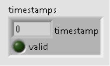
By default the acquisition state machine expects exactly one valid timestamp for each acquired record, which like the triggers, is an input on the Multirecord Acquisition Write Wrapper.vi. This timestamp is used for providing timing information to the host when trigger events occur. For example, it is used when using the High-Resolution Trigger and provides timing information with subsample accuracy. In other trigger modes, the timestamp is not used but is still required and, instead of waiting for the Reference Trigger to send it, it’s sent when the “ready for reference trigger” event is sent from the acquisition state machine.
Figure 8: Screenshot of the Timestamps Cluster Input on niInst Multirecord Acquisition Write I16 Wrapper.vi
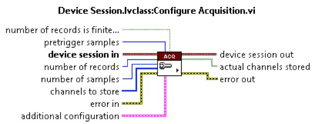
This requirement can be removed or changed through configuration in the Multirecord Acquisition Host IDL. For example, we could configure the acquisition to require zero timestamps per record, and leave the timestamp input unwired on the FPGA. This is configured by using the additional configuration input of Configure Acquisition.vi in the host VI. In the additional configuration cluster, there is a control called timestamps per record. The value written to this control must match the number of timestamps per record provided to the Multirecord Acquisition Write VI. If this control requests more timestamps than provided in the FPGA, then the host code timeouts and no data is sent from the FPGA to the host.
Figure 9: Screenshot of the Host VI Configure Acquisition.vi
Summary of the Multirecord Acquisition Sample Project
To perform triggering in the Multirecord Acquisition example, we must provide the acquisition engine the trigger information as well as record timestamp data (with the default implementation). These are the two required sets of output information from custom trigger implementations that are needed to properly signal the acquisition engine and for the creation and streaming of records from the FPGA to the host.
Creating the Waveform Match Trigger
In this section, we discuss the details in implementing a custom trigger on the NI PXIe-5171R. The triggering IDL created is called the Waveform Match Trigger, which was showcased during the NIWeek 2014 keynote demo announcing the first reconfigurable oscilloscope, the NI PXIe-5171R.
Main Components
To implement this trigger functionality, two FPGA VIs were created, in addition to several host VIs. Here are the details of the VIs created in the Waveform Match Trigger IDL.
Figure 10: NI Waveform Match Trigger IP: Interval Max & Min Hold.vi
The Interval Max & Min Hold.vi in Figure 10 stores the maximum and minimum values of the input waveform (data in) for N samples, where N is the interval length.
Figure 11: NI Waveform Match Trigger IP: Time Mask Trigger.vi
The Time Mask Trigger.vi in Figure 11 compares the past M points of an input waveform received through “data in” to the upper and lower limits (tmt.config). The “data out” from the previously explained Interval Max & Min Hold.vi is used as input waveform for “data in” on this VI. When the waveform falls entirely between the upper and lower limits, the in range output is asserted high. The upper and lower limits are configured serially, with the assistance of the tmt.write config indicating the input limits pair (tmt.config) is valid, and tmt.config done indicating the input limit pair has successfully been added to the upper and lower limit arrays. The number of limits supported, or the array length of the configured limits, is indicated by tmt.resources.
In the next section, we look at how these VIs are implemented and discuss the design decisions made to reach this final implementation.
Implementation Details
To implement the Waveform Match Trigger, we create an array from the user-defined trigger limits/constraints, an array of the min and max limits. This is sent to a set of FPGA registers, implemented as shift registers in LabVIEW FPGA. Once the Waveform Match Trigger IDL is configured and enabled, ADC samples are sent through the pipeline created by the trigger limits. The output from the trigger limits pipeline is then used to drive the Reference Trigger of the Multirecord Acquisition sample project.
The Trigger Limits
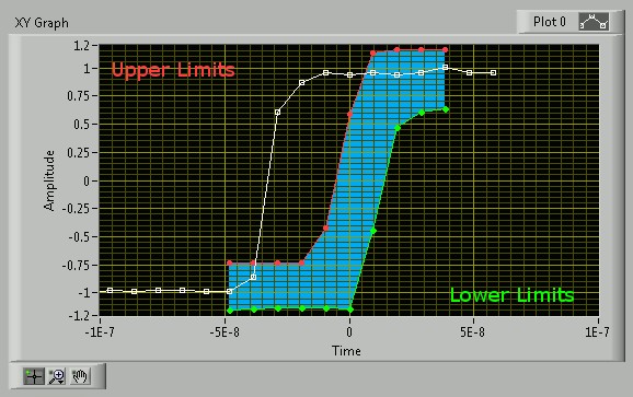
The area defined by these arrays creates a keep-in area, and a valid trigger occurs when all the samples under comparison are found within this keep-in zone as shown in the blue region of Figure 12. Specifically, this IP triggers when all the ADC samples are less than all the upper limits and greater than the lower limits. From now on, we refer to these bounds as the trigger limits or, simply, limits. When we define the limits, they are created in pairs, an upper limit and a lower limit, the limit values themselves being voltage values. The entire trigger limit arrays are composed of these pairs, where the time difference between each set of limits is a constant value (dt). As the samples become available from the ADC, they are compared to the limits. The following animation gives a high-level overview of the Waveform Match Trigger functionality. As the ADC acquires new samples, they are added to the waveform and all the acquired samples shift to the next set of limits to be compared against. Once all the waveform samples are within the keep-in zone/constraints, the trigger condition is met, and a trigger signal is sent to the Multirecord Acquisition Engine.
Figure 12: Animation of Waveform Samples Moving Through User-Defined Trigger Limits
The Limits Pipeline
The trigger limits are implemented in the FPGA as a pipeline that consists of a set of LabVIEW Feedback Nodes connected together serially. With an FPGA pipeline, we can take advantage of the parallel processing capabilities of the FPGA, the code between each Feedback Node running concurrently in the FPGA. For more information on pipelining with LabVIEW FPGA and how data flows through each stage, see the white paper article: Pipelining to Optimize FPGA VIs.
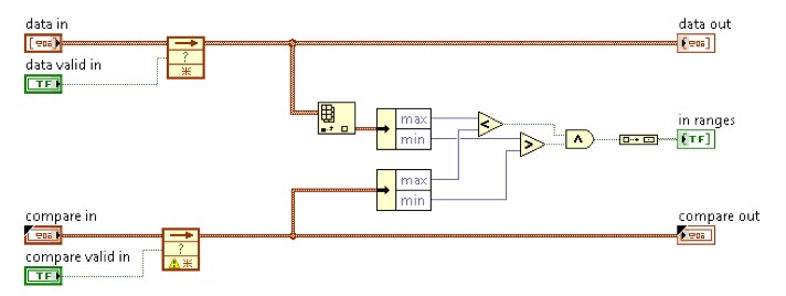
For our Waveform Match Trigger, each stage in the pipeline looks something like Figure 13.
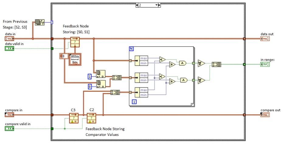
Figure 13: Waveform Match Trigger Comparator (1 SPC) Implementation (FPGA)
The data limits are sent to the hardware one set at a time, and then on the rising edge of the “compare valid in” signal, the limit set is saved into the corresponding Feedback Node. When “compare valid in” is FALSE, the saved value is read out of the Feedback Node, acting like an FPGA register. With multiple instances of Figure 13 implemented and connected together (“compare out” is connected to “compare in” on the next instance, and so on), the effect of writing one limit pair is that the pairs in each Feedback Node are passed to the next implementation, effectively shifting the limits by one down the implemented pipeline.
Data flows through the pipeline in the same way, as it is implemented identically. In Figure 13, the top Feedback Node is part of the data pipeline, and the bottom Feedback Node is part of the limits pipeline. They have separate valid input signals, so the data and the limits can flow through the respective pipelines independently. This is needed because the limits pipeline is filled with the user-defined limits, before we shift any data through, and when we begin shifting the data through the pipeline, the limits are not shifted and remain static.
The Comparator
A comparator as shown in Figure 13 is implemented in each segment of the pipeline and performs the comparisons between the input data and the trigger limits. The output of a single comparator is a Boolean value indicating if the input data is within the limits and is labeled “in ranges.” This output is then combined with each stage of the pipeline and, because there are no Feedback Nodes between the comparator outputs, the aggregated comparator outputs can be evaluated in a single clock cycle to determine if a trigger condition has occurred: the data from ALL comparators are “in range.” This comparison is implemented as a logic AND.
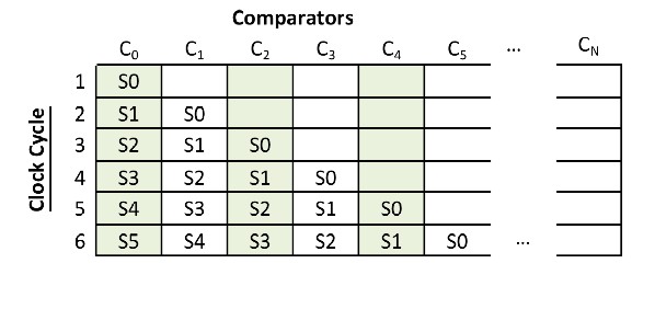
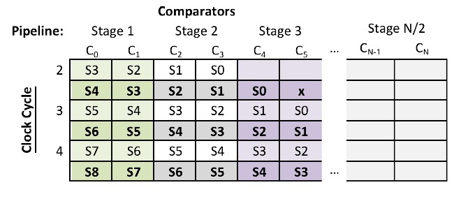
When one sample is generated per clock cycle, then for each clock cycle, we push one more sample into the comparators pipeline. Table 1 shows how the comparator pipeline fills with data one clock cycle at a time. Because all comparators are implemented in parallel, each row is evaluated simultaneously, with empty cells indicating comparisons that are discarded (comparisons with uninitialized values are garbage).
Table 1: Comparator Pipeline (1 Sample per Cycle) Filling With Samples
Comparator Complications: Multiple Samples per Cycle
For the NI PXIe-5171R family, the ADCs generate two samples per cycle (2 SPC) in the data loop on the FPGA. This means that in each clock cycle in the acquisition loop, we have an array of two fixed-point numbers for each channel, instead of one.
Devices that generate more than one sample per cycle (1 SPC) complicate the comparators in the limits pipeline, as we now need more comparators to compare the additional samples and samples between consecutive clock cycles. For N samples generated per cycle, we need 2N comparators to compare each sample generated to each comparator in a given segment.
For the 2 SPC case, two comparators are needed for comparing the first and second sample generated to the first and second comparator in each segment respectively. Another comparator is needed to compare the first sample to the second comparator value. The fourth comparator is needed to compare the first sample from the previous segment to the first comparator in the current segment. This is illustrated in Table 2. Each clock cycle compares the two new samples to the two comparators in each pipeline stage, with the extra comparators comparisons highlighted. Notice how the extra comparators fill in the jumps such that each sample gets compared to each comparator, like the 1 SPC case shown in Table 1.
Table 2: Comparator Pipeline (2 SPC) With Extra Required Comparators Highlighted and Bold (Each Pipeline Stage Is Color-Coded)
Thus, for the 2 SPC case, the following figure illustrates how the limits pipeline and comparators are implemented to handle the extra samples in each clock cycle. Additional notes show how the implementation can be compared to the pipeline in Table 2. The Feedback Nodes have been labeled to indicate the waveform data and limit pairs stored in each, causing it to represents the Stage 2 comparators in Table 2 during the second clock cycle.
Figure 14: Waveform Match Trigger Comparator (2 SPC) Implementation (FPGA)
In Figure 14, the “data in” is an array of clusters with two elements: max and min. The array length matches the number of cycles per sample generated by the hardware. The cluster was implemented this way to support sending either waveform data or summarized data from the Interval Min & Max Hold.vi (which is the default implementation). To represent a single waveform sample, the two values in the cluster are identical. Implementing the data input in this way allows us to summarize multiple waveform samples to send through the limits pipeline instead of each individual sample. In the next section, we discuss this design decision in further detail.
Resource Utilization and the Need for Data Decimation/Summarization
When sending waveform data directly into the limits pipeline, we can test for waveform matches, granular down to the individual samples. Without the ability to summarize multiple waveform samples, the maximum length of our limits array is limited by the number of pipeline segments implemented in hardware, which is fixed at compile and can be very resource intensive, leaving little room in the FPGA for other customizations. With fewer segments, we use fewer resources; however, we also have a smaller window of time in which our unique waveform match event must occur, which is defined by the following equation:
Time Window = Segment Length * Sample Rate Period
Thus, our time window with 512 pipeline segments, with the default sample rate of 250 Mhz on the NI PXIe-5171R is:
512 * 1/250 MHz = 2.05 µS
If our triggering event cannot be described completely within ~2µS, a longer envelope is needed, which in turn requires more segments and more FPGA resources.
To overcome this problem, we can abstract the data flowing into the limits pipeline from representing one data sample per comparator to multiple samples. One way to do this would be to keep track of the minimum and maximum values of a set of N samples. Then, just send the min and max values through the comparator pipeline, thus representing N points with just one set of comparisons, allowing for an elongated time window. This method is implemented in the Interval Min & Max Hold.vi.
Figure 15: Interval Min & Max Hold.vi
For example, if N = 10, we can track the min and max value over 10 samples. Once we have the min and max for the 10 samples, we need to send only these two values through the limits pipeline, giving us a 10x time window of 20.5 uS. The limitation of this design is that all N samples must share the same min and max limit; therefore, we can increase the time window at the expense of time resolution of the mask.
Multirecord Sample Project With Added Waveform Match Trigger
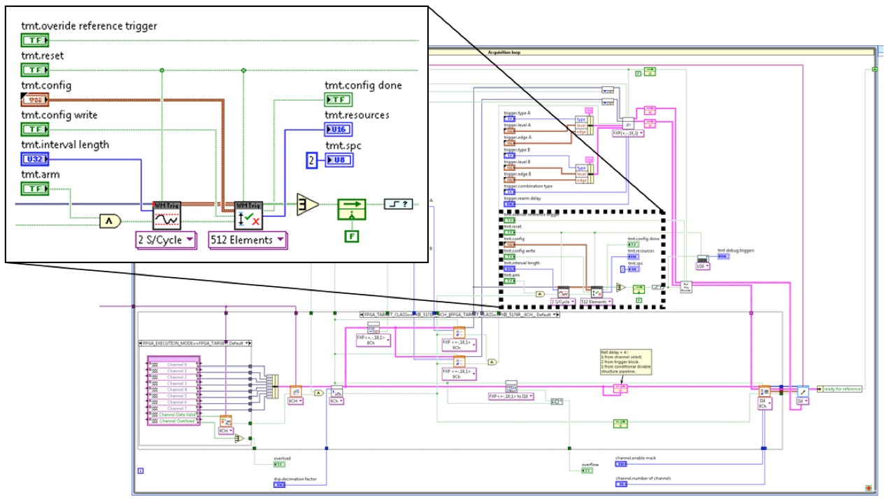
Pulling it all together now, the two new FPGA VIs can be implemented in parallel with the existing trigger functionality to maintain functionality of both trigger types. This is done by overriding the Reference Trigger output from the existing trigger logic with the new Waveform Match Trigger output, conditionally when it is enabled by the user.
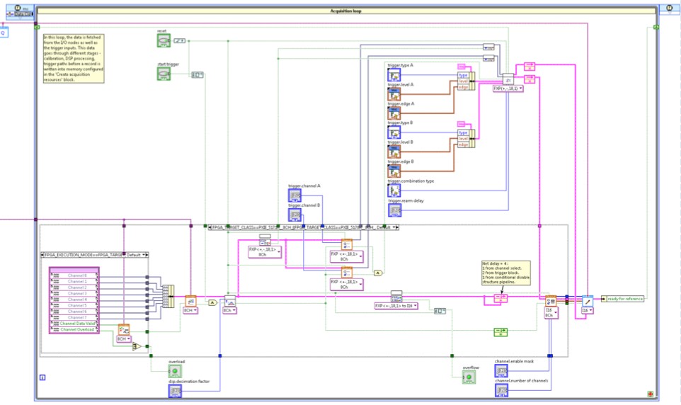
Figure 16 shows an overview of the new Waveform Match Trigger implemented in the Multirecord Acquisition sample project for the NI PXIe-5171R FPGA VI, in parallel with the existing trigger IP.
Figure 16: Screenshot of the Waveform Match Trigger FPGA VIs Implemented in the Multirecord Acquisition Sample Project
Conclusion
We have seen one example on how you can modify the functionality of software-designed instruments to exactly meet the needs of an application. This is very powerful because it adds a lot of flexibility to the instruments. And it is not, of course, limited only to reconfigurable oscilloscopes. You can reuse the code between software-designed instruments such as RF analyzers, vector signal transceivers, high-speed serial instruments, and more.
- Download the code for the Waveform Match Trigger
- Explore more examples and IP
- View PXIe-5171R product details
An NI Partner is a business entity independent from NI and has no agency or joint-venture relationship and does not form part of any business associations with NI.
