The PXIe-5164 Oscilloscope. Maximize Accuracy and Input Range. Minimize Compromise.
Overview
NI introduced the first oscilloscopes to include FPGAs that could be targeted and reprogrammed with the LabVIEW FPGA Module in 2014. This leap forward in instrumentation technology gives you the ability to define the operation of your oscilloscopes to meet your needs now and in the future as your devices and experiments change. The PXIe-5164 oscilloscope gives you unprecedented accuracy, bandwidth, and signal flexibility in a reconfigurable oscilloscope. Learn more about the PXIe-5164 reconfigurable oscilloscope and how it can help you decrease your cost of test, shorten your time to market, and improve your test yield.
Contents
- PXIe-5164 Oscilloscope
- PXIe-5164 Analog Performance
- User-Programmable FPGA
- Key Application Areas
- Product Variants
- Next Steps
PXIe-5164 Oscilloscope
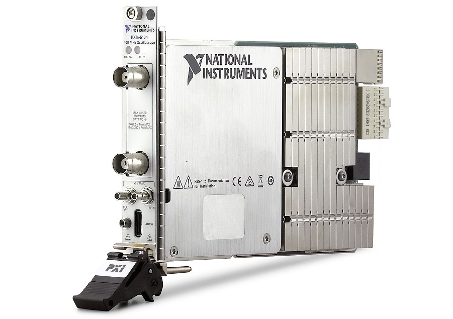
The PXIe-5164 can do the job of multiple oscilloscopes by combining the highest bandwidth, widest input voltage range, and largest offset range for a 14-bit ADC design in any commercial oscilloscope. The PXIe-5164 technology includes:
- Two 14-bit channels sampled at 1 GS/s with 400 MHz bandwidth
- Two Category II-rated channels with voltage input range to 100 Vpp with programmable offsets allowing measurements up to ± 250 V
- Up to 34 channels to build parallel, high-channel-count systems in a single PXI chassis
- A 3.2 GB/s streaming data rate enabled by eight lanes of PCI Express Gen 2 bus communication
- A Xilinx Kintex-7 410 FPGA to create custom IP, including filtering or triggering, programmed through LabVIEW
And with the modularity to meet evolving requirements, this new oscilloscope provides a zero-compromise solution for any test and measurement system.
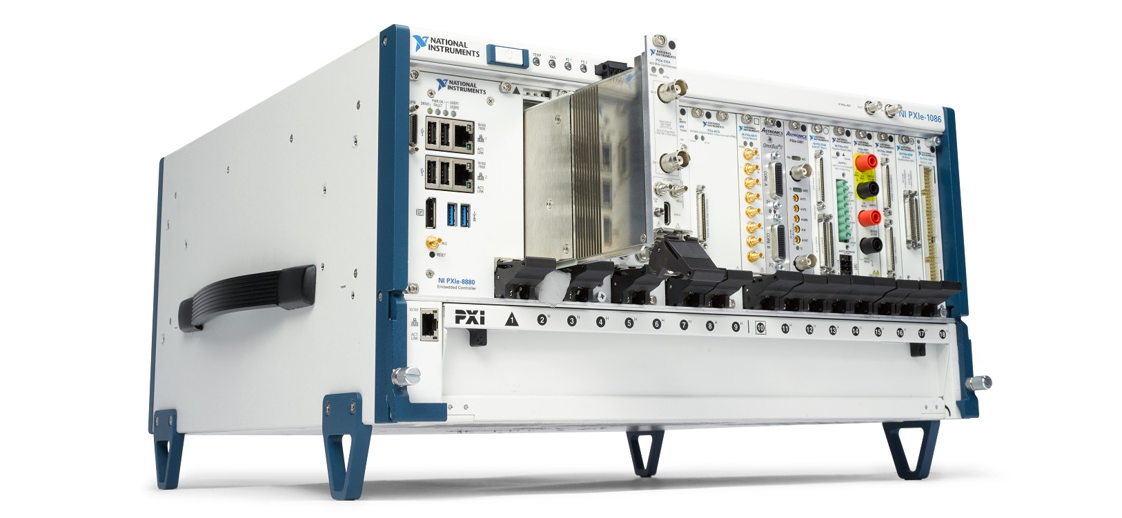
Figure 1. The PXIe-5164 is a no compromises oscilloscope with 400 MHz of bandwidth, 14 bits of resolution, and 250 volts of measurement range.
PXIe-5164 Analog Performance
The art of analog design is often hidden in the specifications. Behind specifications such as bandwidth and effective number of bits (ENOB) are characteristics such as passband flatness, step response, linearity, and noise. PXIe-5164 analog design characteristics include a wide dynamic range analog-to-digital converter (ADC) and analog front end, robust high-voltage design with no loss in high-resolution performance, and the ability to use digital signal processing (DSP) to stabilize and equalize the magnitude and phase responses.
Wide Dynamic Range ADC and Front End
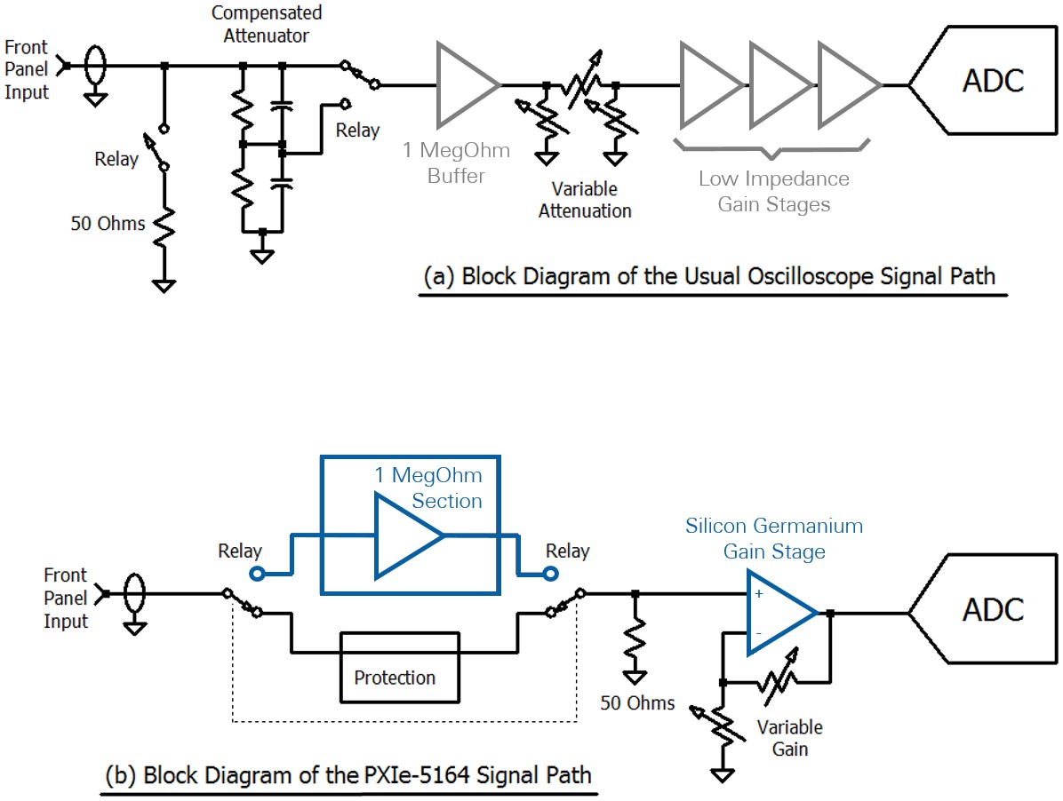
The PXIe-5164 uses a Texas Instruments ADS54J40, an ADC remarkable for its low noise spectral density specification of 155.9 dBFS/Hz. To maintain this low noise floor in an oscilloscope, you need to depart from the usual circuit arrangement. Figure 2(a) shows the block diagram of a typical oscilloscope where the 50 Ohm mode is accomplished by simply connecting a 50 Ohm resistor in parallel with the front panel input. The signal passes through the 1 MOhm buffer which is optimized for high input impedance and high voltage. By necessity, less design emphasis is placed on the noise and distortion performance in the 1 MOhm buffer. Figure 2(b) shows the approach taken in the PXIe-5164 oscilloscope where a dedicated 50 Ohm path bypasses the 1 MOhm section and connects directly to the low-impedance amplifier section. The performance limitations of the 1 MOhm stage are thus avoided. The low-impedance amplifier in Figure 2(b) is a single-stage silicon germanium ADC driver with variable feedback. Using one amplifier rather than several (several stages being characteristic of most oscilloscope designs) eliminates the noise and distortion contributions of the multiple stages. Also, gain control in this single-stage circuit is accomplished by changing the degree of feedback rather than by varying the degree of input attenuation (again, the latter being characteristic of the usual approach). So, the highest level of performance is obtained in the 50 Ohm mode.
Figure 2. The PXIe-5164 oscilloscope has a signal path (b) optimized for measurement accuracy by bypassing the 1 MegOhm buffer on the 50 Ohm path and having only a single gain stage, as opposed to a usual oscilloscope signal path (a) that is optimized for high impedance and voltage.
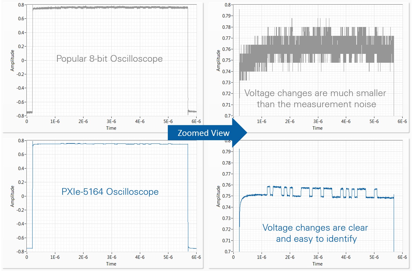
You can most clearly see the superior dynamic range of the PXIe-5164 in side-by-side measurements with a popular 8-bit box oscilloscope. Figure 3 shows time domain plots of a one-time-event communications signal riding on a digital pulse taken with a box scope and a PXIe-5164 oscilloscope. The communications signal amplitude is one percent of the pulse amplitude. Both instruments were set for 50 Ohms on their 2 Vpp ranges. To improve signal-to-noise ratio, the bandwidth of the box scope was reduced to its 250 MHz setting and its acquisition mode was set to high resolution. The communications signal is nearly indiscernible in the data captured with the 8-bit box scope but easily recognizable and decodable in the data captured by the PXIe-5164 oscilloscope.
Figure 3. Compare the time domain plots of a popular 8-bit box oscilloscope with the PXIe-5164 oscilloscope with both sampling an identical one-time-event communications signal riding on a digital pulse. The communications signal is nearly indiscernible on the 8-bit box scope but easily recognized and decodable on the PXIe-5164.
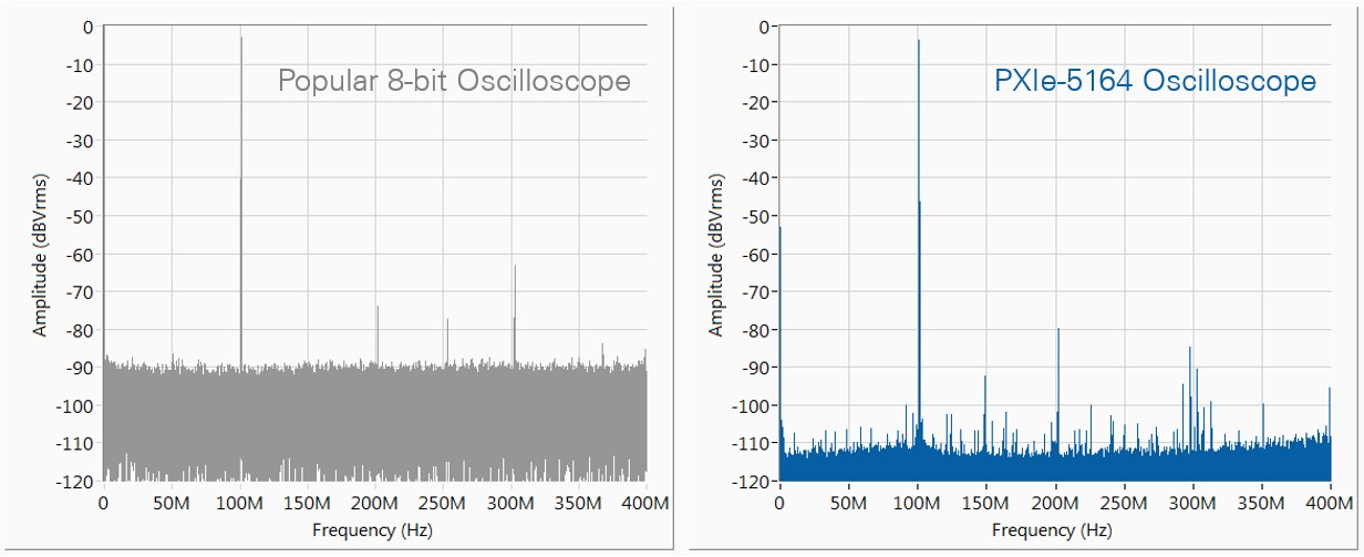
Figure 4 shows spectral results of the same box scope and the PXIe-5164. Input is a 101 MHz sine tone at 11 dBm. Both oscilloscopes were set to 50 Ohms, 2 Vpp range, and full bandwidth with the fast Fourier transform (FFT) number of points set to one million. The noise floor of the PXIe-5164 oscilloscope is an astonishing 22 dB lower. If the size of the FFT of PXIe-5164 data is reduced to 200,000 points so that both FFTs have the same 2.5 KHz bin width (the box instrument samples at 5 Gs/s versus 1 Gs/s for the PXIe-5164), the noise floor difference is still an impressive 16 dB. The PXIe-5164 oscilloscope also has the better harmonic distortion performance.
Figure 4. By comparing the spectral results of a popular 8-bit box oscilloscope with the PXIe-5164 oscilloscope, you can see the noise floor of the PXIe-5164 oscilloscope is an astonishing 22 dB lower.
Robust High-Voltage Design With No Loss in High-Resolution Performance
The simplicity of the 50 Ohm signal path in the conventional oscilloscope affords a high degree of overload protection but compromises performance because the 1 MOhm buffer is included. The PXIe-5164 oscilloscope signal path design overcomes this problem by having a special series protection circuit in the directly coupled 50 Ohm path (the block labeled “protection” in Figure 2[b]). A high degree of protection is obtained without compromising the 50 Ohm performance.
Most oscilloscopes implement high voltage ranges through one or more compensated voltage divider that you switch in and out using bulky electromechanical relays, as Figure 2(a) shows. The relays consume valuable board area that you could use to implement a variety of other necessary oscilloscope functions. The PXIe-5164 oscilloscope avoids this by using a patent-pending technique where all switching is done at low voltage. The PXIe-5164 can measure voltage swings up to +/-50 V on offset voltages up to +/-250 V with no need for problematic electromechanical relays.
DSP Stabilizes and Equalizes the Magnitude and Phase Responses
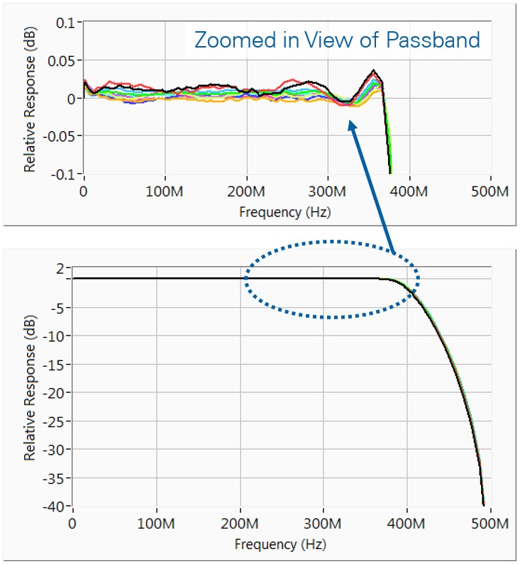
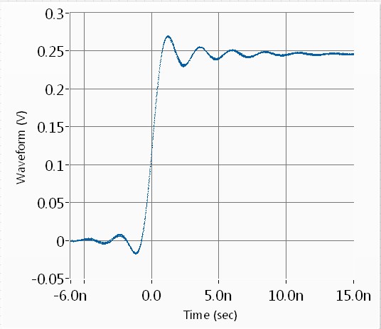
Variability is inevitable in the frequency and step response of an oscilloscope’s analog front end. Digital filtering can offer a considerable improvement in range-to-range, channel-to-channel, and even unit-to-unit variability. Moreover, you can use digital filtering to adjust the response for other characteristics such as passband flatness and linear phase response. In the PXIe-5164 oscilloscope, a 16-tap finite impulse response (FIR) filter is in the FPGA and in line with the ADC data stream to realize these advantages. The filter parameters are determined during factory or external calibration and transferred from EEPROM to the FIR filter depending on range, impedance, and filter setting. The calibration procedure mandates a very flat-with-frequency power meter, hence a guaranteed and traceable flat frequency response is transferred to the PXIe-5164 during calibration. Flatness at +/- 0.5 dB to 330 MHz is guaranteed. Figure 5 shows a typical PXIe-5164 oscilloscope measured response where the deviation from 0 dB is less than 0.022 dB for all ranges and channels. Figure 6 shows a measured step response where symmetry in the waveform indicates the wanted linear phase characteristic.
Figure 5. This graph shows the frequency response of a typical PXIe-5164 oscilloscope on the 50 Ohm path up to the full bandwidth (400 MHz). The response of all ranges and channels of one module are superimposed and the maximum deviation in the passband is 0.022.
Figure 6. PXIe-5164 oscilloscope 50 Ohm step response, full bandwidth (400 MHz). Symmetry in the step response is the result of the minimum phase characteristic imposed by the in-line FIR filter.
User-Programmable FPGA
Whereas off-the-shelf instrumentation hardware traditionally has fixed capability, NI is leading the way in more open, flexible measurement devices based on FPGA technology. FPGAs are high-density digital chips that you can customize to directly incorporate custom signal processing and control algorithms into measurement hardware. The result is off-the-shelf hardware that has the best of both worlds—fixed, high-quality measurement technology; the latest digital bus integration; and user-customizable logic that is highly parallel, provides low latency, and is tied directly to I/O for inline processing and tight control loops.
FPGAs continue to gain design wins and market share from application-specific standard products (ASSPs) and application-specific integrated circuits (ASICs) because they keep up with Moore’s law better than other devices and dramatically lower development costs. This results in smaller test system size and lower power consumption. Very capable FPGAs are entering the market and defining the hardware capabilities of many devices, but the IP they contain is vendor defined and the FPGA’s power may be inaccessible to you. This is largely because the specialized hardware description language (HDL) knowledge needed to program these devices requires a steep learning curve and is generally restricted to digital design experts.
LabVIEW software makes the latest FPGA technology accessible. Using graphical programming, you can implement logic to define the behavior of an instrument in hardware and reprogram the instrument when requirements change. The graphical dataflow nature of LabVIEW is well suited for implementing and visualizing the type of parallel operations that can be implemented in digital hardware.
Software-Designed Instrumentation Versus Traditional Instruments
User-programmable FPGAs in your measurement system hardware provide benefits that range from low-latency device under test (DUT) control to CPU load reduction. The following sections describe various usage scenarios in more detail.
Improve Test System Integration With Onboard Decision Making
In many test systems, you must control the DUT or chip under test through digital signals. Traditional automated test systems can sequence through DUT modes and take the needed measurements in each stage. In some cases, automated test equipment (ATE) systems incorporate intelligence to progress between DUT settings according to the measurement values received.
In either scenario, software-designed instruments that incorporate a user-programmable FPGA result in cost and time savings. Consolidating measurement processing and digital control into a single instrument reduces the need for additional digital I/O in the system and avoids configuring triggering between instruments. In cases where the DUT must be controlled in response to measurement data received, software-designed instrumentation closes the loop in hardware and reduces the need for decision making in software at a significantly higher latency.
Decrease Test Time and Increase Confidence With In-Hardware Measurements
Today’s software-based test systems can perform a limited number of measurements in parallel, but software-designed instrumentation is limited only by the available FPGA logic. You can process dozens of measurements or data channels with true hardware parallelism, removing the need to choose between measurements of interest. With software-designed instruments, functionality such as real-time spectral masking is achieved with dramatically higher performance and at a fraction of the cost compared to traditional boxed instruments.
The low latency associated with performing measurements in software-designed instruments means that you can take tens or hundreds of live measurements and average them together in the same amount of time as a traditional test system requires to take a single measurement. This results in improved test-result quality and increased confidence in your measurements.
Focus Only on Interesting Data With Custom-Defined Triggers
Traditional instrument options for low-latency trigger behavior are fixed according to the hardware being used, but with software-designed instrumentation you can incorporate custom triggering functionality into your device to quickly zero in on situations of interest. Flexible hardware-based triggering means that you can implement custom spectral masks or other complex conditions as criteria for either capturing important measurement data or activating additional instrumentation equipment.
See a custom trigger built with LabVIEW and implemented on a software-designed oscilloscope in a 5-minute webcast or read about the implementation.
Reduce CPU Processing Loads With Real-Time Onboard Signal Processing
Processing large amounts of data can tax even the most capable commercial CPUs, resulting in systems with multiple processors or extended test times. With software-designed instrumentation, you can preprocess data in hardware, potentially reducing the CPU load significantly. Computations such as FFTs, filtering, digital downconversion, and channelization are implemented in hardware, reducing the amount of data passed to and processed by the CPU.
Gain Confidence in Final Design Performance With Rapid Prototyping
You traditionally use instrumentation just for test and measurement applications, but the connectivity between I/O and software in modular instruments gives you the ability to prototype electronic systems using instrumentation. For example, you can prototype advanced radar systems using digitizers and RF signal analyzers; the connectivity to a user-programmable FPGA allows quicker advanced algorithm deployment in prototype and faster proof-of-concept validation.
Key Application Areas
The PXIe-5164 oscilloscope is built on the open, modular PXI architecture and includes a user-programmable FPGA to help you in many application areas, including aerospace/defense, semiconductor, and research/physics, that require high-voltage measurements and high levels of amplitude accuracy. The user-programmable FPGA provides the highest level of flexibility, performance, and future-proofing currently possible with off-the-shelf hardware. As your system requirements change, software-designed instruments preserve your software investment across different pieces of modular I/O and ensure you can modify your existing I/O according to the application at hand.
Figure 7. The PXIe-5164 oscilloscope is a powerful addition to modular test systems for aerospace and defense built on the PXI platform.
Aerospace and Defense Test
The lifespan of many aerospace and defense testers can reach 40 years and beyond. The challenges of replacing an obsolete instrument and recertifying a tester can be extremely costly. The high voltage range of the PXIe-5164 oscilloscope and reconfigurable nature of the instrument make it a good choice for the go-to oscilloscope in new designs, as well as a drop in replacement for obsolete instruments. Because many specifications or characteristics, such as triggers or filters, need to stay consistent through the generations of testers, this new oscilloscope helps to alleviate backward compatibility issues that may arise by allowing you to reuse the hardware IP created in LabVIEW, helping to reduce both certification and maintenance costs.
See where NI is making an impact in the aerospace and defense industries.
Energy Research
The energy community values many channels that are synchronized on a common bus to provide high-resolution acquisitions across a wide range of input voltage levels. With the PXIe-5164, you can easily synchronize PXI modules in a chassis (the PXIe-5164 oscilloscope can support 34 channels in one chassis) or multiple chassis using NI-TClk or additional timing and synchronization modules. The high voltage range reduces the need for additional attenuation of vast signal types that are inherent with tests that address PDV, plasma, or tokamak applications. Additional applications include partial discharge monitoring and analysis that benefit from both the high input voltage range and the user-programmable FPGA to perform and process measurements at hardware speeds.
Learn about how NI is improving operations and advancing research in the energy industry.
Semiconductor and Automotive Test
The increase in smart automotive ICs has driven increased voltage requirements in the test of semiconductor components for the automotive industry. Devices that operate at high voltage and high frequency are becoming more and more common in tomorrow's smart vehicles. Additionally, the high resolution of the PXIe-5164 oscilloscope is necessary for viewing noisy bus communication to and from the engine control unit, such as SPI or CAN, and the test of other subsystems require higher voltage input requirements than traditional high-resolution solutions currently offer.
Product Variants
NI offers a lower performance variant of the PXIe-5164 for applications that need the wide voltage range, high resolution, and low noise performance but not necessarily the bandwidth or user-programmable FPGA.
| PXIe-5163 | PXIe-5164 |
Channel count | 2 | |
Resolution | 14 bits | |
Voltage range | 100 Vpp input range (with offset, ±250 V max) | |
Sample rate | 1 GS/s | |
Bandwidth | 200 MHz | 400 MHz |
Programmable FPGA | N/A | Kintex-7 410 |
Onboard memory | 512 MB | 1.5 GB |
Next Steps
- Explore the PXIe-5164 oscilloscope to see detailed specifications, choose accessories, and purchase your new oscilloscope.
- Shop all NI oscilloscopes to choose the right one for your application.
- Learn about the fundamentals of oscilloscope operation and performance in the Instrument Fundamentals series.
