More Throughput vs. Less Latency: Understand the Difference
Overview
Contents
- What does it take to get a single measurement into an algorithm?
- What are Throughput and Latency?
- Improving throughput
- Improving Latency
- Sample Use Cases
- Links and Further Reading
In most measurement or control applications, the goal is to get real world data from a signal into some logic or algorithm. Before software became readily accessible, such applications were implemented completely in hardware - often analog circuits. While some applications continue to use custom, dedicated hardware implementations for their algorithms, today the majority of control or measurement algorithms are implemented in software. Software allows drastic simplification and reduction of implementation, design iterations, and testing. It also allows for more abstraction, to simplify the level of working detail to a manageable scope.
The design of one of these measurement and control systems focuses on getting a signal from the physical world into the algorithm, which is in software.
What does it take to get a single measurement into an algorithm?
Let's first look at what it takes to get a single, one-point measurement from the physical world into a software algorithm.
Figure 1: Measurement and Control systems are built around the goal of getting a measurement from the signal into an algorithm.
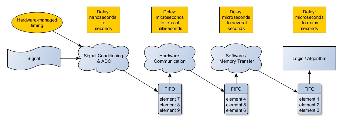
As with all processes, this is not instantaneous. The major delays can be grouped into three categories.
• First is signal conditioning and analog to digital conversion. This is concerned with turning the physical signal into a digital electronic signal. There may be filters or other processes here. Even the fastest digital to analog converters (DACs) have a maximum speed, due to physical limitations.
• Second, there is hardware communication. This includes all the processes necessary to get the signal off of the DAC and onto the software execution system, such as a PC. The largest portion of this is bus latency.
• The third delay is software specific, and includes any software or memory transfer needed to get the signal into the correct memory and deliver it to the algorithm. This can involve DMA read operations, processing interrupts, and other operations such as copying the data into the algorithm.
Figure 2: The three general classes of delay
To quantify these, sample rates can be as slow as about 1 second per sample on some slow, high precision devices. On the other hand, there are devices that can sample in the GS/s range. Hardware communication ranges from on the order of microseconds all the way to tens of milliseconds, depending on the bus and the architecture of the system. Software processing and memory transfer are driven by the speed of the software, and can vary widely based on the performance on the processor as well as the design of the software.
Finally, there is the time it takes to complete the algorithm before a result is available. This calculation could be a simple task such as PID control or buffering and writing it to disk, or it could involve more advanced calculations such as computation of differential equation-based simulation models.
So the path from signal to algorithm can be broken down like this:
Figure 3: The three general classes of delay, and their respective timing.
What are Throughput and Latency?
Latency is the amount of time it takes to complete an operation. It is measured in units of time, and is often found in units of milliseconds, microseconds, and nanoseconds. In many applications such as control applications, what is important is round-trip latency. That is the time from an input to its corresponding output. In this case, the signal must travel not just up the chain to the algorithm, but back down the chain again to a digital to analog converter where the physical signal can be output.
Throughput is the rate at which the system can process inputs. It is an amount of measurements per a given time. It is not a measure of how recent they are, rather just a measurement of their volume. Throughput is commonly expressed a samples per second (S/s), though it is useful to note that many computer components are rated in B/s, MB/s, GB/s, etc. Those components play into the total throughput of the system. One common synonym is the term bandwidth.
After seeing how one measurement can go from signal to algorithm, how can it be done faster? There are two ways to do this, with two different results. One is to improve the throughput, and the other to reduce latency.
Improving throughput
The way an operation is timed can critically affect the throughput. There are two ways to time the acquisition of a measurement. The first is software timing: it requires input from the computer to control the acquisition, and the timing is managed in the software. Since the computer software provides the command, for it to happen multiple times successively would require the software to loop through and the same steps. In addition, most of the delay is dominated by the software-controlled parts of the process.
Figure 4: Software timed acquisition
Then there is hardware timing, which is used in conjunction with First In, First Out buffers (FIFOs). Hardware clocks on the chip take samples at precise intervals and push them into the buffers and up the chain. This can be used to increase the sampling speed. It also allows each operation to pass a group of data points instead of a single data point, saving overhead and making the operations more efficient. This concept, depending on where it is applied, can be called array operations, buffered operations, vector operations, or batch operations. In this way, more samples can be processed at a time, and the time between samples can be reduced.
Hardware timing and buffers are advantageous because the overhead of going through each of these processes is incurred for each batch of samples, and not for every sample. That way, even though a hardware communication may take place once per ten samples, if ten samples are sent each time, then the sampling rate can be ten times that of the hardware communication rate.
Figure 5: Hardware timed acquisition, using FIFOs and hardware timing to increase throughput
What this has done here is not speed up the rate at which the system iterates as a whole. Rather, it has pushed more data through it in a given time. As far as the sampling rate goes, it effectively lets the software latency time be divided by the number of items in our buffer. It is the major advancement that improved what is today the software-timed max rate of a jittery 100 to 150 samples per second to the GS/s rates of the fastest devices. That is an improvement of 6 or 7 orders of magnitude.
Buffers and hardware timing are centered on improvements to throughput, and not do not help reduce latency. In fact, the extra buffers may hurt latency.
Improving Latency
There are a few technologies that address improving latency. The two main tools around this goal are the Real Time operating system and the FPGA.
Real Time Operating Systems
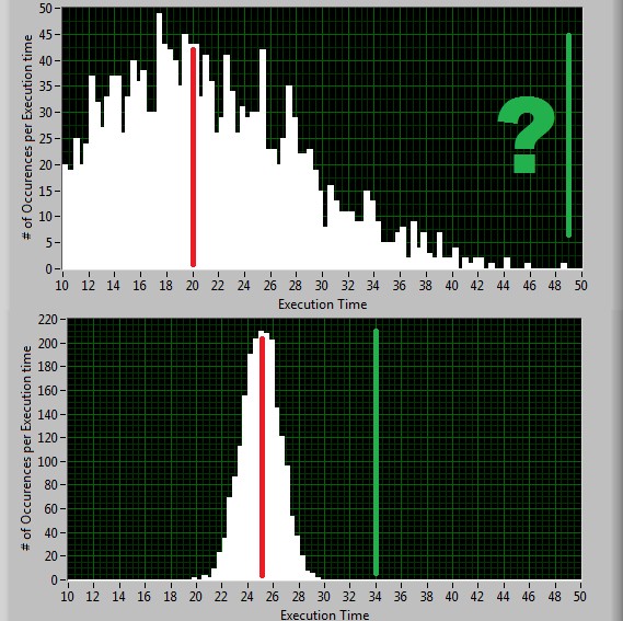
Any operating system will experience jitter, or variation in latency. Normal operating systems, such as Windows, are designed to run all programs as fairly as possible. In order to promote this fairness and time sharing, there is often jitter in a given program as the operating system cycles through running other processes. Jitter can take the form of pauses that last for a handful of milliseconds, or even be as large as tens of seconds. If in certain circumstances, the jitter can be practically unbounded. This jitter limits the usefulness of general purpose operating systems when it comes to executing a task with a high degree of regularity. That is because they are designed for fairness, not for repeatability, and a given task will have a wide variation in execution time.
A Real Time operating system (RTOS) is not designed for fairness but for repeatability, by limiting jitter. Examples of these include Pharlap, VXWorks, and RT Linux. The architecture of the operating system has the goal of making a given operation execute in a regular amount of time. That way, the time it takes to execute a task is very predictable and regular, with very little jitter.
With the extra effort to reduce jitter, there are operations on an RTOS which on average take longer to execute than on a general purpose operating system. However, the practical upper bound of the execution time can be much lower.
Figure 6: Simulated loop times for a control loop running on two operating systems. TOP: A general purpose OS has loop times that vary widely, with no practical upper bound (green line). BOTTOM: A Real-Time OS has a higher average (red line), but less jitter. This lets it be used dependably at higher rates.
General purpose operating systems are unfit to be applied in many applications with timing requirements, because of their high jitter. But with a Real Time operating system, a PC can be deployed into the situation where it otherwise could not be, since its execution time is more regular. Even though the average execution time is longer, the statistical spread is narrower and thus more predictable. The net effect is the increased capability of the PC architecture into applications where it could not otherwise be deployed.
While the RTOS increases the PC’s usefulness by limiting the variation in latency, it does not lower its average latency. In situations where a drastically lower latency is desired, a RTOS is insufficient.
Learn more about real-time operating systems (RTOS)
FPGAs and Latency
There is another set of tools that have been developed to reduce latency. FPGAs, or Field-Programmable Gate Arrays, are made of a hardware “fabric” of elementary nodes. These nodes can be linked together by software to define their behavior, and easily reconfigured. The FPGA brings the benefits of extremely precise timing and reliability that hardware offers, as well as the ease of software development.
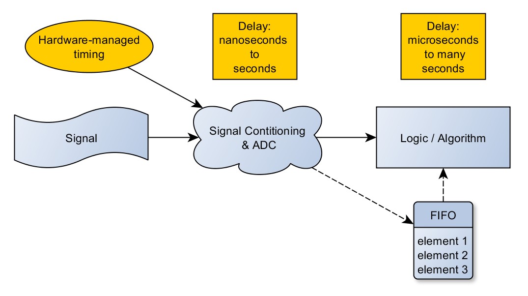
Putting our algorithm on the FPGA shortens the trip from signal to algorithm. On the FPGA the two major delays are the ADC sampling and the computation of the algorithm. In addition, the algorithm is much quicker because it lies in the hardware fabric of the FPGA instead of in a software execution system. It has the flexibility of software since no physical changes need to happen to the device to change its behavior, but has the speed of hardware, executing at clock rates up to (currently) the megahertz range.
Figure 7: FPGA architectures and the shorter trip to the algorithm (showing the optional use of buffers)
Buffers in FPGA applications are optional - and often are only included for computations that require them, such as FFTs. FPGA code without buffers is the architecture most often chosen for the lowest latency applications, where the result is needed as quickly as possible after the input is given. Applications like this tend to deliver a result as soon as possible for output, as in high speed control systems.
FPGAs and Throughput
Although not mentioned in the previous section, FPGAs are also a useful tool to achieve high throughput processing. High throughput processing is possible on an FPGA because the algorithms are executed in hardware. Often, preprocessing steps such as filtering or FFTs or signals are run on an FPGA, and the data is then buffered and passed to a host PC.
What if I want both high throughput and low latency?
It is worth noting that most changes that improve throughput often negatively affect latency. What increases latency can also negatively affect throughput. To achieve a high degree of both concurrently can be met, but usually only with dedicated hardware or FPGAs. The fortunate thing is that most applications need one or the other, and not a high degree of both.
Sample Use Cases
- I want to log vibration measurements from a test cell. I have over a dozen channels of strain, and I wish to sample at a speed of at least 50 kHz. With NI hardware, this might be approached by using a DAQ device, such as the C Series NI-9237 or the PXI-4497.
For this application, samples are taken at a high rate, well faster than could be achieved with software timing. This is an example of a system that has a requirement for high throughput. As long as all of the data arrives in the log file, it is not of critical importance when that happens. Latency, therefore, is not a major concern. When selecting hardware based off of these requirements, throughput will be the primary requirement. An FPGA will not be critical, but high throughput, channel count, sampling speed, and disk space will be necessary. With NI hardware, this might be approached by using a DAQ card, such as the C-series 9237 or the PXI 4497.
- I want to run model-based control for a UAV, and the fastest of these loop times need to execute at the sub-millisecond level. This loop depends only on one sensor, but it is critical to the stability of the craft that it executes with that timing.
There are not many channels involved, and although the sampling rate will need to be higher than software timed rates, throughput is not the main concern. The main concern is delivering an output in time to meet the inherent timing requirements. So, this is an example of an application that requires very low latency. As a result, low latency hardware, perhaps such as an FPGA, will be required. If I were to approach this application, I would likely begin with a Single-Board RIO.
- I want to emulate an RF channel. I have a 4x4 MIMO signal, and want to have a system simulate my transmission channel. I want the test to run live.
This system will have to acquire data, process it, and return results in a very strict time interval. It will also have to handle a very high rate of samples on multiple channels. This is an example of a high throughput and low latency application. The demands on the hardware will be strict, and it will almost certainly require dedicated hardware or a powerful FPGA. With NI hardware, this could be done using the NI vector signal transceiver (VST), the latest of which features 1 GHz of instantaneous bandwidth, or with an NI vector signal analyzer (VSA) with an accompanying FlexRIO FPGA coprocessor.
- I want to simulate a flight dynamics model for my aircraft, so I can use it to test my flight controller. I have hundreds of sensors and actuators, and my model needs to execute at a rate of at least 1 KHz for fidelity.
This simulation system will have tight timing requirements for results to be delivered in. It also has high throughput, because of such a high channel count. This application, then, requires both high throughput and low latency. With NI hardware, this can be met with a high-speed PXI Express controller, such as the PXIe-8135, and suitable I/O modules, some of them including FPGAs.
- I want to acquire a set of pressures and temperatures to monitor the environment at my facility. The rates will not be in excess of one sample a second, and I expect little variation between each sample. With those values, I will do some logging, and alarming if the values go out of range.
This application does not have high throughput, since the data rates are slow. It also does not have strict timing needs, so it does not have a need for low latency. Software timing will be sufficient for this application. The requirements for the hardware are not strict, and a variety of low cost options are feasible.


