High Throughput Multiply
- Updated2025-01-28
- 8 minute(s) read
Computes the product of x and y.
This function supports only scalar and array values of the fixed-point data type.

Dialog Box Options
| Parameter | Description |
|---|---|
| Fixed-Point Configuration |
Specifies the encodings, word lengths, and integer word lengths of the input and output terminals of this function. The configurations you specify determine the value range of the terminals.
|
| Execution Mode |
Specifies how this function executes.
|
| Pipelining Options |
Specifies options for pipelining this function internally. These options affect the maximum clock rate this function can achieve. Refer to the Improving Function Performance by Pipelining section of this topic for information about this relationship.
You can choose from the following options:
|
| Registers |
Specifies whether to add internal registers for function output terminal. This section is available only if you select Inside single-cycle Timed Loop. Note Adding registers can reduce the length of the combinatorial path, which can prevent compilation errors that result from a long combinatorial path. However, adding registers also increases the latency of this function, which means this function takes additional clock cycles to return a valid result.
|
| Optional Terminal |
Specifies a setting for displaying an optional block diagram terminal.
|
| Configuration Feedback |
Displays information about how this function executes. This information is based on the configuration options you specify. |
Inputs/Outputs
 x
—
x
—
Specifies the multiplicand.
y
—
Specifies the multiplicand. Specifies whether the next data point has arrived for processing. Wire the output valid output of an upstream node to this input to transfer data from the upstream node to this node. To display this handshaking terminal, select the Inside single-cycle Timed Loop option and perform either of the following actions:
Specifies whether downstream nodes are ready for this node to return a new value. The default is TRUE. Use a Feedback Node to wire the ready for input output of a downstream node to this input of the current node. Note If this terminal is FALSE during a given cycle, the output valid terminal returns FALSE during that cycle.
To display this terminal, select the Inside single-cycle Timed Loop option and perform either of the following actions:
 x*y
—
x*y
—
Returns the product of x and y. Returns TRUE if the theoretical computed value exceeds the valid range of the output data type. If operation overflow returns TRUE, the Overflow mode option determines the value this function returns. LabVIEW displays the operation overflow terminal only if you place a checkmark in the Operation overflow checkbox. This checkbox is located in the Optional Terminal section of the configuration dialog box. Returns TRUE if this node has computed a result that downstream nodes can use. Wire this output to the input valid input of a downstream node to transfer data from the node to the downstream node. To display this terminal, select the Inside single-cycle Timed Loop option and perform either of the following actions:
Returns TRUE if this node is ready to accept new input data. Use a Feedback Node to wire this output to the ready for output input of an upstream node. Note If this terminal returns FALSE during a given cycle, LabVIEW discards any data that other nodes send to this node during the following cycle. LabVIEW discards this data even if the input valid terminal is TRUE during the following cycle.
To display this terminal, select the Inside single-cycle Timed Loop option and perform either of the following actions:
|
During the cycles before output valid returns TRUE for the first time, this function might return different results on an FPGA target than on a host computer. The results become identical after the first time output valid returns TRUE.
Improving Function Performance by Pipelining
You can improve the timing performance of this function on an FPGA target by adjusting the Number of pipelining stages. The functionality of a pipelined multiplier is equivalent to a non-pipelined multiplier cascaded by a certain number of registers. The number of registers is equal to the number of pipelining stages.
In general, increasing the Number of pipelining stages also increases the maximum clock rate this function can achieve. However, the actual clock rate depends on many factors, including the following ones:
- The FPGA target you use
- The size of the multiplier
- The rounding and overflow modes you select
- The Implementation resource you select
- Other FPGA logic besides the multiplier
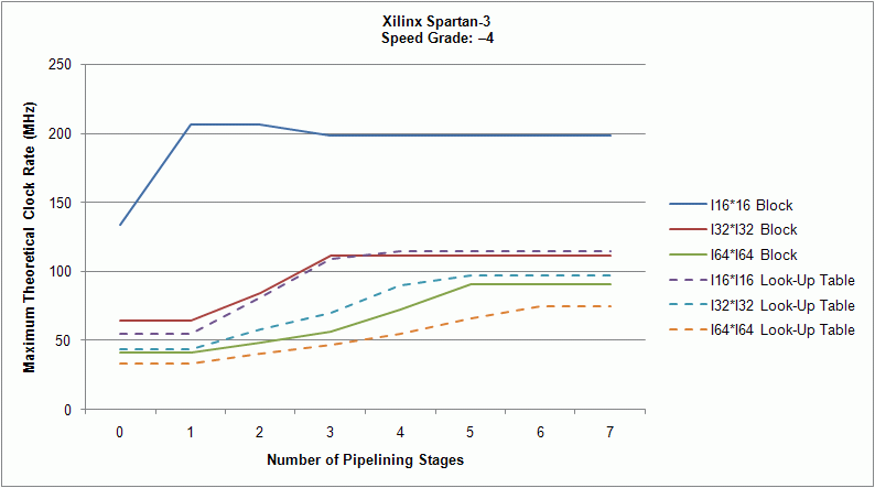
The following graphs show the Number of pipelining stages vs. maximum clock rate estimations on Xilinx Virtex-II, Virtex-5, and Spartan-3 FPGA targets, respectively.
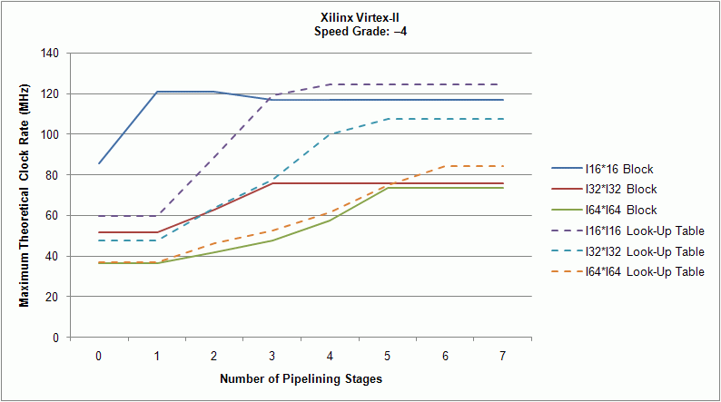
In the previous figure, each line represents a multiplier of a certain size that uses a particular Implementation resource. For example, the I32*I32 Block line shows a multiplier that multiplies two 32-bit signed integers together by using an embedded block multiplier. The result is a signed 64-bit integer: <+/–,32,32> * <+/–,32,32> = <+/–,64,64>. If you use one pipelining stage on a Virtex-II FPGA target, this type of multiplier can achieve a maximum clock rate of about 51 MHz. If you use three pipelining stages, the maximum clock rate becomes about 76 MHz.
The following figures show similar information for other FPGA targets.

Examples
Refer to the following example files included with LabVIEW FPGA Module.
- labview\examples\CompactRIO\FPGA Fundamentals\FPGA Math and Analysis\High-Throughput Math\Vector Normalization\Vector Normalization.lvproj
- labview\examples\R Series\FPGA Fundamentals\FPGA Math and Analysis\High-Throughput Math\Vector Normalization\Vector Normalization.lvproj