Using The SLSC Architecture To Add Additional Elements To The Signal Path Of A Test System
Contents
- Introduction
- Following The Signal Path From Output to Input
- Theory of Operation
- Overview of the SLSC Architecture and Module Development Kit
- Description of Hardware System Components
- Software
- Conclusion
- Appendix 1: Hardware System Components
- Appendix 2: References
Introduction
When building test systems many times the signal path from the Device Under Test (DUT) to the measurement device requires additional elements for custom signal conditioning, loading and switching. It was with this in mind that NI created the NI Switch Load and Signal Conditioning (SLSC) architecture. This document shows how the NI SLSC can be used to add additional elements to the signal path in a typical test system.
As an application demonstration, we will excite an electronic control unit (ECU) with a Pulse Width Modulation (PWM) signal as is commonly used on Electronic Control Units (ECUs) and measure its response. Since many ECUs require higher voltage levels we will add additional elements to perform level shifting to generate and measure a signal referenced to an external power supply like a car battery.
We will also add a relay to insert a fault into the signal path simulating a broken wire in the ECU harness.
The system will use an NI PXI R series FPGA board to generate and measure the digital PWM signal in a PXI chassis, and then scale voltages and add the switch in the SLSC chassis.
For simplicity in this paper, we will not use a real ECU. Our DUT in this case will be a connector block which will wrap the cable around and use one of the digital inputs on the R series to measure the PWM signal generated by the digital output.
Following The Signal Path From Output to Input
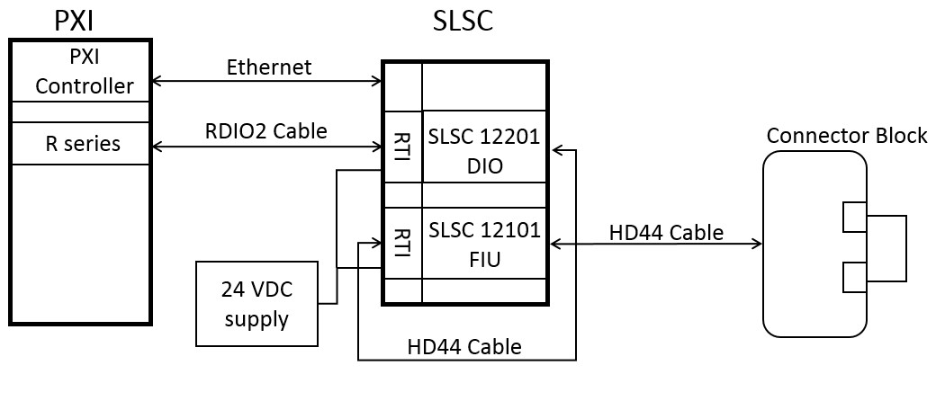
The following diagram shows the signal path which we will follow starting from the PXI system routing through the SLSC to the connector block where the signal wraps around and goes back through the SLSC to the PXI system.
The PXIe-7822R module connects to an RTI-12301 using a standard SHC68-C68-RDIO2 Cable. The RTI-12301 breaks out the signals for the SLSC-12201 Module. The SLSC-12201 is used to scale the signals with respect to an external reference source. In this case we are using a 24V supply but in the real world this could represent the battery voltage on an automotive ECU or aircraft LRU. The signal wraps around from the front of SLSC to the rear using an HD 44 cable and plugs into an RTI-12305. The RTI-12305 breaks the signals out for the SLSC-12101 which is used to switch the signal simulating a broken wire in the harness.
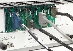
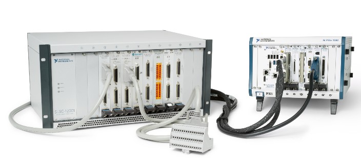
The follow pictures show a rear and front view of the setup which includes additional PXI and SLSC modules which are not used in this application. The wrap back wire, external reference and Ethernet cable are not shown wired in these pictures. The following section describes the signal path in more detail showing the path from PWM output to PWM Input.
Image 4. Rear view of the SLSC
Image 5. Front view of the SLSC and a PXI system.
Theory of Operation
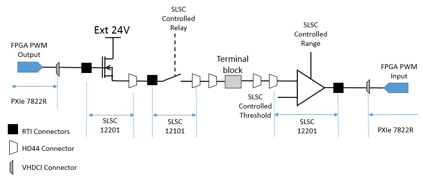
The PWM signal is generated in the FPGA, the FPGA code is shown in the software section. The output pin on the FPGA is available on the VHDCI connector on the front panel of the PXIe-7822R, this signal is a 3.3 Volt signal. The pulse train is transmitted through an SHC68-C68-RDIO2 VHDCI Cable to the RTI-12301 Rear Transition Interface on the SLSC chassis.
The SLSC Module Development Kit specifies a standard way to distribute the signals from the RTI to the SLSC module.
The pulse train is then amplified by the SLSC-12201 module which can convert it to voltages between 5 V and 33 V based on the external Vsup. The SLSC-12201 module is programmed via the ethernet port using the SLSC API and it has a variety of modes in which it can operate. In this case we have programmed the output to be a sourcing output and we have specified it to use an external reference connected to the Vsupp pin on the RTI-12301. For this example we are using an external 24 V DC power supply.
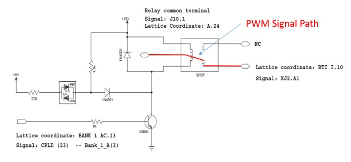
The signal uses Pulse Width Modulation (PWM) with range between 0 V and 24V. This output signal is available on the HD44 connector on the front of the SLSC-12201 module. The signal is wrapped around using a 1:1 HD44 cable to the RTI-12305 and is made available to an SLSC-12101 Prototyping module. On this module we have placed a relay which is controlled using one of the software controlled pins on the SLSC 12101 controller (CPLD).
When the relay is energized the signal is able to pass through the relay and is available on the HD 44 connector on the front of the SLSC-12101 module. The signal is transmitted through a 1:1 HD 44 cable to a connector block where it is wrapped around to the input.
The return path is similar but there is no relay on the SLSC-12101 module, the signal is simply wired through and passed around to the SLSC-12201 which is configured in input mode and with a threshold of 12 V before being scaled back to a value which can be read by the FPGA.
Overview of the SLSC Architecture and Module Development Kit
SLSC Architecture
The SLSC is a modular architecture which complements the NI hardware platforms, PXI and C Series in that it is designed to make it easy for customers and partners to create custom circuit cards needed for test systems which can easily interface from both a hardware and software perspective.
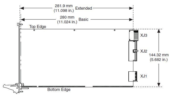
The SLSC architecture consists of three components, the chassis, the module and the Rear Transition Interface (RTI). For details on the chassis please refer to the getting started manual. As shown in the diagrams below the modules are144.32mm tall (4U) by 281.9mm deep with three interfacing connectors on the rear (XJ1, XJ2 and XJ3). The XJ1 connector is used for module communications using the SLSC driver API, the XJ2 connector is for signal interfacing and XJ3 is used for high power connections.
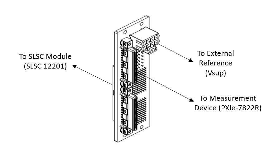
The Rear Transition Interface (RTI) allows for connectivity from the SLSC modules to the NI measurement hardware. Applications may choose from a variety of NI and 3rd party RTI’s or may design your own. Designing your own RTI’s allows the system designer to reduce cabling connectivity and point to point wiring in systems.
The diagram below shows the connections for the RTI to the external reference, the measurement device and to the SLSC-12201 module.
SLSC Module Development Kit
The SLSC Module Development kit (MDK) provides detailed design constraints for designers to achieve system interoperability with other modules and ecosystem products. In order to build modules, the user must have access to a valid MDK kit from NI. For more details on procuring the MDK please contact NI.
Description of Hardware System Components
PXIe Chassis with LabVIEW 2015 and PXIe-7822R
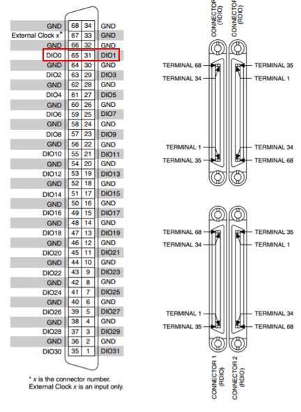
The PXIe-7822R is a reconfigurable I/O (RIO) device that features a user-programmable FPGA for onboard processing and flexible I/O operation. With LabVIEW FPGA, you can individually configure the digital lines as inputs, outputs, counter/timers, PWM, encoder inputs, or specialized communication protocols. You can also program custom onboard decision making that executes with hardware-timed speed and reliability. For this project we are using DIO0 as the PWM out and DIO1 as the PWM in.
SLSC-12201
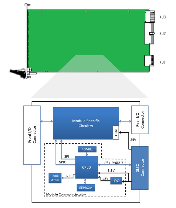
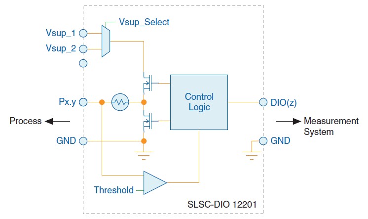
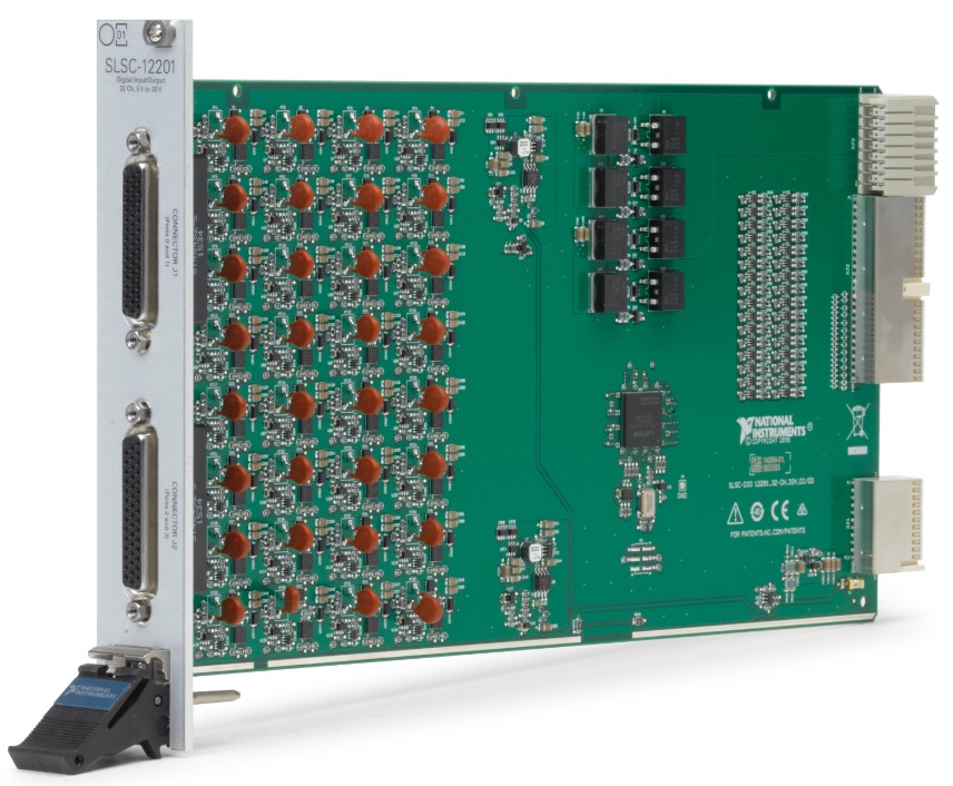
The SLSC-12201 is a digital signal conditioning module designed to work with NI Digital Input and output (DIO) devices. The following is a block diagram and a picture of the module.
The module is configurable via the SLSC bus to either be an output or an input. As an output it is able to amplify digital signals based one of two external references (Vsup_x), the output circuitry can also be programmed to operate in 3 modes: push, pull, or push and pull.
As an input the module defaults to pull-down however it is possible to configure an programmable pull up. The input signal threshold is programmable to operate as a standard 5 V TTL input or an extended range with programmable threshold.
The external reference (Vsup_x) can be programmed to one of two banks of 8 channels each.
For this configuration we are using Vsup_1 which is tied to 24V on the JR1 connector on the RTI 12301 connector.
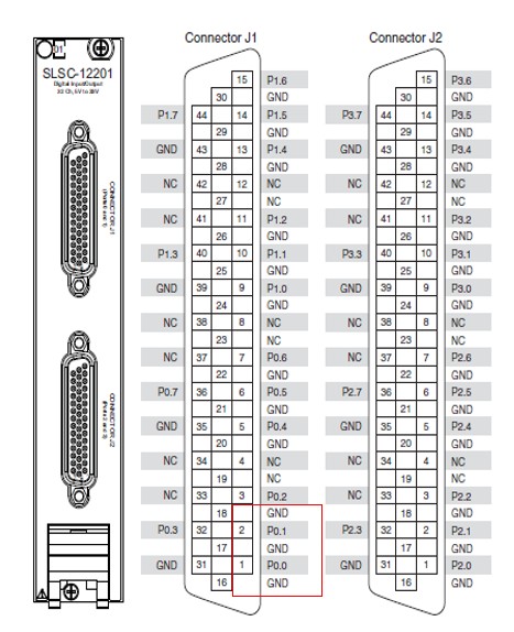
For this project we are using P0.0 as the scaled PWM output and P0.1 as the scaled PWM input.
RTI-12301
The RTI-12301 is used to map the signals from the PXIe-7822R module using a standard SHC68-C68-RDIO2 Cable to the SLSC-12201 module. This maps the PXIe-7822R DIO0 on the PXIe-7822R to P0.0 on the SLSC-12201 module and maps DIO1 to P0.1.
SLSC-12101
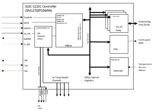
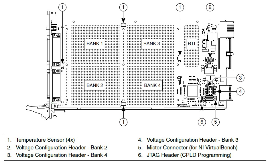
SLSC-12101 is a prototyping module intended to help SLSC module developers quickly prototype designs. The module is divided into 4 lattice areas where users can build prototype circuits by either soldering components directly on the lattice or mounting a secondary circuit card onto the lattice area.
The module observes all the requirements to meet Level 2-compatibility as defined by the SLSC Module Design Specifications and is routed in such a way that it can also reach Level 1-compatibility if the module developer follows the signaling requirements of a Fully Compatible Rear I/O. These requirements are described in Chapter 11 of the SLSC Module Design Documentation.
The prototyping module has 4 lattice banks which can be used for prototyping as shown in the picture below:
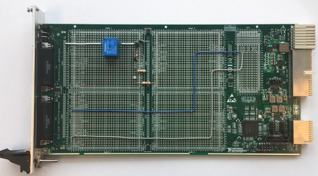
For this example, we have built the circuit shown below on the bank 1 lattice area. The purpose of this circuit is to open or close the SPDT relay simulating an open circuit for our PWM signal. The relay requires 24 V at 15 mA to energize the relay which is supplied by 2N3904 NPN transistor. The transistor is turned on using CPLD pin 23.
The following is the pin mapping used on the SLSC-12101
XJ2: Pin a1 = Scaled PWM output Signal+ » J1 Pin1
XJ2: Pin b1 = Scaled PWM output Signal- » J1 Pin 16
XJ2: Pin d1 = Scaled PWM Input Signal+ Return » J2 Pin3
XJ2: Pin e1 = Scaled PWM Input Signal- Return » J2 Pin18
RTI-12305
The RTI 12305 is used to map the signals from an SLSC using a 44pin connector from the front panel of the SLSC module. This is used for wrap around connections like fault insertion or switching.
External Power Supply, HD 44 Cables and HD 44 Connector Blocks
External power is supplied using a 24DVC power supply from NI (PSU 15) and the signals are cabled using 1 to 1 HD 44 cables to a Phoenix HD 44 connector block.
Software
The software for this project is divided into three sections: the first section shows the programming required for the SLSC-12201, the second section shows the LabVIEW code required to create the PWM signals and the third, how to use the SLSC-12101 for fault insertion.
Programming the SLSC-12201
Description of Module Capabilities
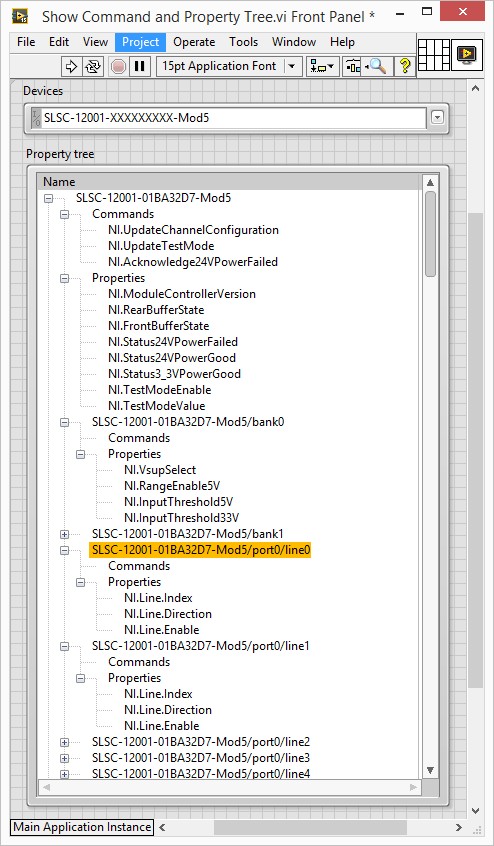
Each SLSC Module is configured by properties and commands which are divided between Module capabilities and Physical Channel capabilities. These capabilities are stored in Non-Volatile Memory (NVMEM) on the module which removes the need to install a special software layer to use the module. The SLSC API allows you to control the module features.
Using the "Show Command and Property Tree.vi" shipping example allows the user to obtain all the properties and commands for the SLSC-12201 module.
Programming the SLSC-12201
The first step is to configure the direction of line 0 of port 0 to a digital output, this is the path for PWM output:
The next step is to configure the direction of line port to a digital input, this is the path for the digital input:
The following code assigns Vsup_0 to bank 0; Vsup_0 is connected to the external 24V supply. The VI also sets the high/low threshold to 12V.
Notice that this code uses the Command NI.UpdateChannelConfiguration. This will commit all of the previous setup properties and it will enable all of the configuration of the digital channels and banks at the same time.
Programming the PXIe-7822R
PWM Output
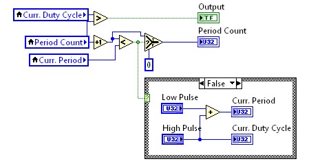
The following LabVIEW FPGA code shows a how to generate a PWM output signal:
PWM Measurement
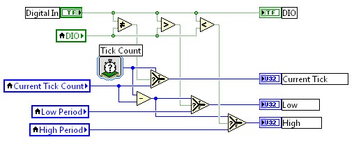
The PWM input is measured using this following diagram. For details on building PWM firmware for the NI R series devices see this link: http://www.ni.com/example/5963/en/
Programming the SLSC-12101 and Host Application
Disconnect Switch
This code controls the relay and it can insert open circuit faults whenever the user desires or whenever the test suite programs. This code below uses an event structure (to avoid generating unnecessary traffic to the SLSC chassis):
Host Application
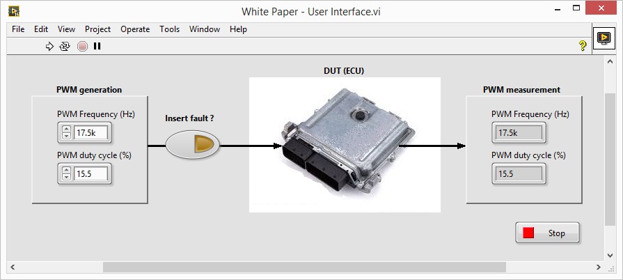
The final system will for this simple application can be seen below. This shows the LabVIEW front panel.
Conclusion
This document demonstrates how to use the SLSC architecture to add additional components to the signal path of a test system using the NI SLSC architecture.
Appendix 1: Hardware System Components
The following is a list of hardware and software parts used:
Item | PN | Name | Description | Manufacturer | Qty |
1 | 781622-01 | PXIe-1078 | PXIe 9 Slot Chassis | NI | 1 |
2 | 783003-04 | PXIe-8840 | PXIe Controller with Windows 64 bit | NI | 1 |
3 | 783486-01 | PXIe-7822R | PXIe R series FPGA Module | NI | 1 |
4 | 156166-01 | SHC68-C68-RDIO2 Cable | Shielded R Series High Speed Digital Cable, 1m | NI | 1 |
5 | 784532-01 | SLSC-12001 | 12-Slot SLSC (System Load and Signal Conditioning) Chassis | NI | 1 |
6 | 785369-01 | RTI 12301 | RTI DIO 32 FOR SHC68-C68-RDIO2 Cable | NI | 1 |
7 | 785356-01 | SLSC-12201 | SLSC-12201 33V DIO module with thresholding | ||
8 | CS-DSDHD44MF0-005 | HD44 Cable | 44-Pin (HD44) Deluxe HD D-Sub Cable - Copper Shielded - Male / Female | Amphenol | 2 |
9 | SET Part number | RTI-12305 | RTI-12305 FOR HD44 connector | SET | 1 |
10 | 785204-01 | SLSC-12101 | Prototyping module | NI | 1 |
11 | 781093-01 | NI PS15 | External 24V power supply | NI | 1 |
12 | Part No: 2322427 | HD44 Connector block | Phoenix Contact HD44 Connector block MFG | Phoenix Contact | 1 |
Appendix 2: References
- SLSC Module Design Documentation (available from NI with purchase of PN 785205-01)
- SLSC-12001 Getting Started Guide and Specifications
- SLSC-12201 Getting Started Guide
- SLSC-12101 User Guide
- Pulse Width Modulation Example DAQ Personality


