Identify and Characterize Damaging PCB Assembly and Test Processes Using Strain Gage Testing
Overview
Stress-induced solder joint failure is one of the most common modes of printed circuit board assembly (PCBA) failures. Today, this problem is further exacerbated with the introduction of lead-free solder material, which, for similar tensile and compressive strengths, is almost twice as brittle as the traditional tin-lead solder. Various assembly and test processes can cause solder joint failures on PCBAs by over-flexing them even before they are shipped out. This white paper explains how you can use the IPC/JEDEC-9704 guideline and NI hardware and software to characterize strain and identify problematic designs and processes.
Contents
- Problem Statement
- PCB Strain Gage Tests
- Step 1: Select a Strain Gage
- Step 2: Prepare PCB for Test and Mounting Strain Gages
- Step 3: Measure Strain
- Step 4: Analyze and Report Data
- NI Solution for PCB Strain Gage Testing
- Results at NI
- Conclusion and Next Steps
Problem Statement
Engineers have been using PCBs and PCB-based products for decades, so why is stress-induced failure a growing issue today? In an attempt to answer this question, experts on this topic have examined how predominant trends in the electronics industry during recent years impact maximum allowable stress limits on PCBs. Two of the most relevant trends are:
- Greater use of lead-free solder instead of the traditional tin-lead solder
- More frequent use of compact ball grid array (BGA) components
Reasons for the above trends and their associated benefits are obvious. The Restriction of Hazardous Substances (RoHS) directive took effect in the European Union in July 2006. This directive restricts the use of six hazardous materials, including lead in the manufacture of various types of electronic and electrical equipment. The downside of this is that most of the lead-free solder alternatives have higher brittleness, and when it comes to assembly and test processes during manufacturing, the lead-free solder is more prone to cracks than the traditional tin-lead solder when subjected to stress.
BGA components offer many advantages over surface-mount packages including higher density of pins, better heat conduction and prevention of overheating because of its lower thermal resistance, and superior electrical performance because of the short distance – and thus lower impedance – between the package and the PCB. On the flip side, BGA components present some disadvantages including expensive inspection, reduced responsiveness to thermal expansion, and higher flexing and vibration compared to surface-mount components with longer leads. BGA components are not very efficient at evenly distributing stresses, and are more prone to solder ball joint cracking, specifically on the inner rows.
Each of the above two trends individually lowers the limit on maximum mechanical stress that can be directly applied to a PCB. When combined, they dramatically increase possibilities of solder joint cracks if maximum allowable stress is exceeded and almost make it mandatory to characterize the boards and surrounding equipment for maximum stress levels. Assembly and test processes like in-circuit test (ICT), depanelizing, or final verification test (FVT) involve holding the board in some form of a fixture and then performing a task. If these fixtures are not designed properly, they tend to apply higher than safely allowed stresses on the PCBs. Even well-designed fixtures tend to apply higher stresses over time on the PCB inside.
To proactively avoid failures and identify problematic designs or processes, you can implement a strain gage test on the PCB to characterize these potential high-stress-inducing processes for maximum stresses and make sure they are within the allowed limits. If measured stress values exceed the maximum allowable stress level for the board, you can rework or redesign the fixture or change the process as required to bring these values within allowed limits. The IPC/JEDEC-9704 guideline identifies problematic assembly and test processes and provides systematic steps for implementing a PCB strain gage test.
IPC (originally founded as the Institute for Printed Circuits and now known as IPC: Association Connecting Electronics Industries) is a global trade association dedicated to the competitive excellence and financial success of its 2,600 member companies that represent all facets of the electronics interconnect industry, including design, PCB manufacturing, and electronics assembly. IPC and the Joint Electron Device Engineering Council (JEDEC) released two guideline documents in 2004/2005 regarding mechanical stresses on PCBs. IPC/JEDEC-9702 is a strain characterization guideline and IPC/JEDEC-9704 focuses on printed wiring board strain gage tests.
Download a full copy of the IPC/JEDEC-9704 guideline from the IPC Web site.
Download a full copy of the IPC/JEDEC-9704 guideline from the JEDEC Web site.
In the following sections of this white paper, learn about the four PCB strain gage testing steps as recommended by the IPC-9704 guideline.
PCB Strain Gage Tests
With PCB strain gage tests, you can quantitatively assess and characterize potential high-stress-inducing and damaging processes, but you need to identify these processes first to implement the tests. According to the IPC/JEDEC-9704 guideline document, the manufacturing steps typically characterized are:
- SMT assembly process
- Board depanelization (routing) processes
- All manual handling processes
- All rework and retouch processes
- Connector installation
- Component installation
- Board test processes
- In-circuit test (ICT)
- Board functional test (BFT) or equivalent functional test
- Mechanical assembly
- Heat sink assembly
- Board support/stiffener assembly
- System board integration or system assembly
- Peripheral component interconnect (PCI) or daughter card installation
- Dual in-line memory module (DIMM) installation
- Shipping environment
Although ICT and BFT are typically the highest strain/strain-rate operations in the above list, damage is possible in any other process, and you should implement strain tests on as many processes as possible.
Once you have identified the processes, you can implement the following four steps of a PCB strain gage test:
- Select a strain gage sensor
- Prepare the PCB for test and mounting strain gages
- Measure strain
- Analyze and report data
Step 1: Select a Strain Gage
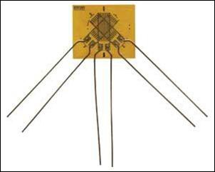
A strain gage is a device whose electrical resistance varies in proportion to the amount of strain in the device. The IPC/JEDEC-9704 guideline document recommends using three-element stacked rosette strain gages for PCB strain gage tests.
A rosette strain gage (Figure 1) consists of three independent strain gages stacked on top of each other. Unlike a wire strain gage, which can measure strain in only one direction, a rosette strain gage measures the full state of strain on the surface of a part. In other words, you can measure not only the two extensional strains, ex and ey, but also the shear strain, gxy, with respect to some given x-y axis system.
Figure 1. Three-Element Stacked Rosette Strain Gage
Assuming that the x and y axes are specified, you can mount two gages in the x and y directions to measure the associated extensional strains in these directions. However, there is no direct way to measure the shear strain, gxy. Nor is it possible to directly measure the principal strains because the principal directions are not generally known.
The solution to this problem lies in recognizing that the 2D state of strain at a point (on a surface) is defined by three independent quantities that you can take as either (a) ex, ey, and gxy or (b) e1, e2, and q, where case (a) refers to strain components with respect to an arbitrary xy axis system and case (b) refers to the principal strains and their directions. Either case fully defines the state of 2D strain on the surface and can be used to compute strains with respect to any other coordinate system. This situation implies that you should be able to determine these three independent quantities if you can make three independent measurements of strain at a point on the surface. The most obvious approach is to place three strain gages together in a “rosette” with each gage oriented in a different direction and with all of them located as close together as possible to approximate a measurement at a point. If you know the three strains and the gage directions, you can solve for the principal strains and their directions or, equivalently, the state of strain with respect to an arbitrary xy coordinate system. The relations needed are the strain transformation equations, and Mohr’s circle construction provides a good visualization of this process.
According to the IPC/JEDEC-9704 guideline, details of the recommended strain gage are as follows:
- Three-element stacked rectangular (0/45/90) rosette strain gage
- 1.0 to 2.0 mm,2 nominal, gage sensor size
- 120 or 350 W strain gages
- Lead wire attach pads located at or lead wires attached on one side of strain gage
Several companies provide three-element stacked rosette strain gages, for example Kyowa (KFW-D17, a waterproof triaxial foil strain gage) and Vishay (C2A-06-062WW-350 or C2A-XX-062LR-350, a general-purpose rectangular rosette strain gage).
Step 2: Prepare PCB for Test and Mounting Strain Gages
Because only a limited mechanical strain is applied prior to surface-mount technology (SMT) reflow and, more importantly, because solder joints are formed only after reflow, strain characterization is required only for assembly and test operations following SMT reflow. Typically, a minimum of two test boards are instrumented. They are not required to be electrically functional, but they must mechanically represent the latest design.
Data suggests that stress-related failures occur at CBGA components. The IPC/JEDEC-9704 guideline recommends that you measure any BGA device with a package body size equal to or larger than 27 by 27 mm. For example, you should characterize tape BGA, flip chip BGA, enhanced BGA, ceramic BGA , and low standoff BGA components that meet this requirement.
This includes selecting the location at which you are going to mount the strain gages. If there is no space to mount a strain gage on the board, you might have to make space on the PCB by removing already mounted components on the test board.
Board preparation is a critical part of the instrumentation process. Proper board preparation helps ensure the proper bonding of strain gages; this, in turn, improves reading accuracy. You also should perform strain gage attachment in accordance with instructions the strain gage and adhesive suppliers provide. Note that strain gages require the use of specially formulated adhesive systems, and strain gage suppliers typically provide this information. You can find additional details about board preparation, strain gage attachment, and wire routing in the IPC/JEDEC-9704 guideline document.
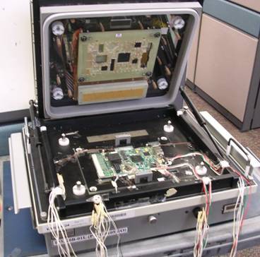
NI is a manufacturer of test, measurement, and control hardware and software equipment, with most of the hardware products being PCB-based. NI implements PCB strain gage test on the products it produces according to the IPC/JEDC-9704 guideline, specifically on the lead-free products with BGA components sized 27 by 27 mm or larger. Figure 2 shows an example of a test board at NI with strain gages mounted and ready to undergo ICT.
Figure 2. Test Board with Strain Gages Mounted in an ICT Fixture
Step 3: Measure Strain
After preparing the board and mounting the strain gages, the third step in PCB strain gage testing is connecting the sensors to data acquisition instrumentation and running the actual test. The length of the test may vary – it can typically run for 5 to 10 seconds while data is recorded. IPC/JEDEC-9704 recommends paying attention to the following parameters while running the test:
- Scan frequency (sampling rate)
- Sampling resolution and gain setting
- Number of channels
- Simultaneous sampling
- Excitation voltage
Scan Frequency
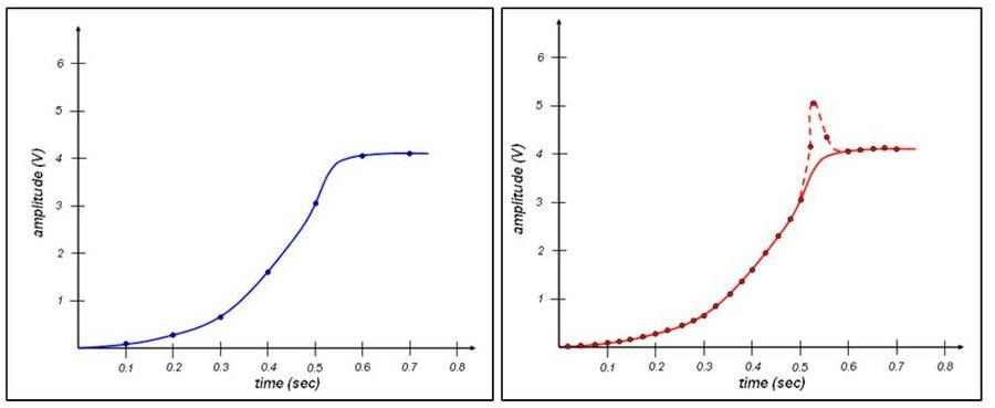
Scan frequency, or sampling rate, is the rate at which data is sampled in the units of number of samples per second (Hz). For PCB strain gage tests, a minimum scan frequency of 500 Hz is recommended, although typical scan frequencies range from 500 Hz to 2 kHz. This sampling rate ensures the capture of any high-frequency dynamic events that may occur. For example, consider measurements at two different frequencies as shown in Figure 3. When sampled at 4X the frequency, Figure 3(b) shows a voltage peak that was not captured with a slower sampling frequency in Figure 3(a).
Figure 3(a) and (b): Example with Two Different Sampling Rates
Sampling Resolution
Sampling resolution refers to the number of bits of the analog-to-digital converter (ADC) in the data acquisition hardware. The higher the resolution, the smaller the input signal changes that can be detected and the more accurate the measurement. For PCB strain gage tests, a minimum sampling resolution of 12 to 16 bits is recommended. ADCs also have a gain setting (the factor by which the signal is amplified), and setting the appropriate gain value ensures making the most of available bits of resolution on the data acquisition hardware.
Number of Channels
The number of available monitoring channels limits the number of measurements in one pass. At least 12 measurement channels are required to monitor four stacked rosettes mounted at all corners of a BGA chip, and at least three channels are required to measure one stacked rosette. While you can make multiple passes if there are insufficient channels, you must monitor all three gages in any stacked rosette at the same loading to avoid any strain calculation errors during analysis.
Simultaneous Sampling
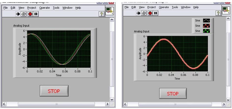
You must monitor all three gages in a stacked rosette at the same loading and in the same pass. The data acquisition device you use dictates how you take these measurements. Two of the common techniques are multiplexing and simultaneous sampling. Data acquisition devices that offer multiplexing feature one ADC and sample channels sequentially. For PCB strain gage tests, sequential sampling may result in miscalculated strain values. Data acquisition devices with simultaneous sampling offer an individual ADC per channel, resulting in measurements taken on all channels at the exact same time and eliminating any errors in strain calculations.
Figure 4. Sequential versus Simultaneous Sampling
Bridge Completion and Excitation Voltage
Each of the three individual gages in a stacked rosette is a quarter-bridge gage that requires bridge completion and excitation voltage – both of which are provided by the data acquisition instrumentation – to function.
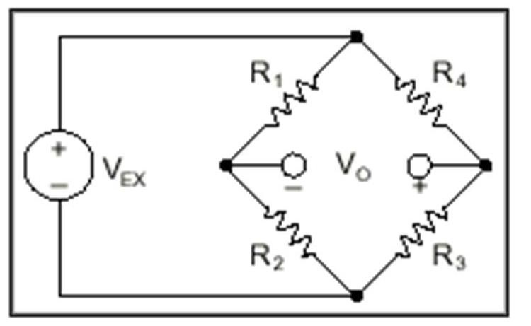
Bridge completion for a quarter-bridge strain gage sensor includes providing three of the four arms of a Wheatstone bridge (Figure 5), where the gage acts as the fourth arm.
Figure 5. Wheatstone Bridge
Because the PCB material has low thermal conductivity, gages are more likely to heat up due to the electrical current passing through them. While using a three-lead-wire setup and quarter bridge reduces this effect, you should balance the excitation voltage with the signal-to-noise ratio (SNR). If the strain value drifts significantly while the board is at rest, reduce the voltage until this effect either disappears or the SNR becomes acceptable. In general, an excitation level of 2 V should provide satisfactory performance.
Step 4: Analyze and Report Data
Once you have acquired the raw strain data, you can begin the last step of the PCB strain gage test – analyzing this data to calculate resultant stresses (maximum and minimum) induced on the board during the test. You can complete this analysis online during the test or offline after the test has finished and you have collected all of the data.
Analysis details vary with the particular strain limit criteria you are using. Many strain limit criteria may require obtaining strain rates or principal strain calculations using Mohr’s circle equations. According to the IPC-9704 guideline, at a minimum, you should provide the peak values of the principal or axial strain (maximum and minimum) for each step monitored.
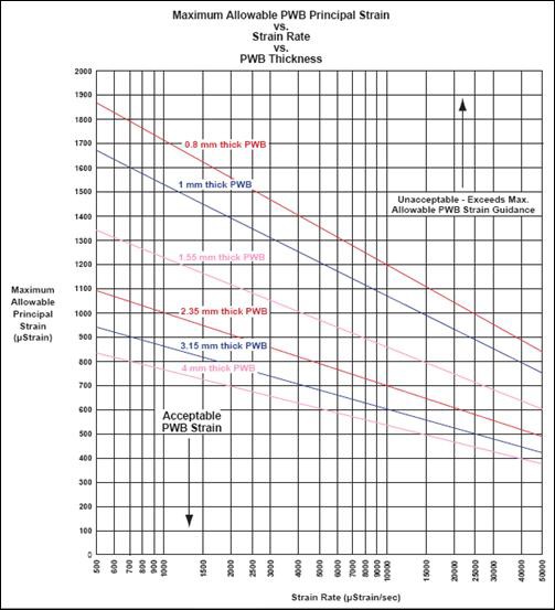
A common way to report data is with a strain versus strain-rate chart, where the y-axis represents maximum allowable principal strain (ustrain) and the x-axis represents strain rate (ustrain/second). Strain rate is the change in the absolute value of strain between consecutive readings. An example of a strain versus strain-rate chart is shown in Figure 6 (courtesy of the IPC/JEDEC-9704 guideline).
When you do not need to analyze the data online, you can export the data to disk and store it in a suitable file format for offline analysis.
Figure 6. Example Strain versus Strain-Rate Chart
NI Solution for PCB Strain Gage Testing
With more than 40 years of experience in test and measurement, NI is a global market leader in PC-based data acquisition with a complete family of data acquisition products for desktop, portable, industrial, and embedded applications. As analog, digital, and bus technologies have evolved, NI has consistently incorporated them in its products. Today, NI offers a variety of data acquisition and sensor measurement platforms for different needs based on measurement types, channel counts, desired resolutions, and other key requirements.
The NI C Series and PXI hardware platforms are designed for voltage, current, and sensor measurements. Each of these platforms includes strain specific measurement modules ideal for measuring strain gages. When you combine NI hardware with NI LabVIEW software, you create a flexible and modular PCB strain gage test system.
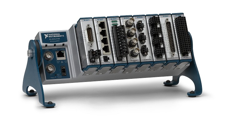
C Series is a family of 3.4 by 2.7 by 0.9 in. I/O modules that are interchangeable within our CompactDAQ and CompactRIO hardware platforms. The NI 9237 four-channel strain/bridge measurement module is recommended for PCB strain gage tests. It offers 24-bit resolution and 50 kS/s per-channel sampling rate, both well over recommended specifications.
Figure 7. NI 9237 C Series Module within a CompactDAQ Chassis
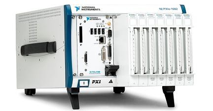
The PXI platform includes 6.3 x 3.9 x 1 in modules that are housed in a rugged chassis that can range from 4 to 18 slots. The backplane of the chassis includes built-in timing and synchronization buses for precision timing and triggering. There are over 1500 module types on the PXI platform, including the eight-channel NI PXIe-4330 and NI PXIe-4331 bridge modules with 24-bit resolution. For most PCB strain gage tests, the PXIe-4330 is sufficient with a 25 kS/s/ch sample rate, but the PXIe-4331 with 102.4 kS/s/ch is available when very high sample rates are required. The PXI platform is recommended for the highest performance strain measurements.
Figure 8. NI PXI Express 8-Slot Chassis
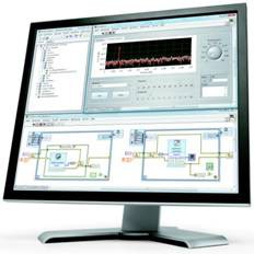
LabVIEW graphical programming software is designed for the development of scalable test, measurement, and control applications. It offers a seamless interface to data acquisition hardware through the easy-to-use NI DAQ Assistant and powerful NI-DAQmx driver software. Apart from the more than 700 built-in analysis functions, LabVIEW includes core data structures such as arrays and clusters and core programming building blocks like loops, case structures, and state diagrams, extending its capability to address virtually any application. Because of its graphical approach, intuitive user interfaces for making any types of controls and indicators, for example, strain versus strain-rate strip charts, are inherent to LabVIEW.
Figure 9. NI LabVIEW Graphical Programming
LabVIEW combines data acquisition, analysis, and reporting in a single software environment, making it an extremely compelling tool for PCB strain gage testing.
NI offers several hardware options for strain measurements, including C Series and PXI. Each of these solutions is based on NI-DAQmx driver software and use the same LabVIEW API, so you can easily move from one platform to another with minimal or no changes to existing software as your channel-count need grows.
NI DIAdem software is designed for managing, analyzing, and reporting data collected during data acquisition and/or generated during simulations. The offline analysis and reporting capabilities of DIAdem make it a perfect tool for quick access to the large volumes of data collected during PCB strain gage tests, for consistent reporting, and for data visualization.
Results at NI
With strain verification and monitoring program using systems based on C Series and LabVIEW, NI has been successful in avoiding strain-related failures and field returns. NI produces more than 500 unique hardware products, most of which are PCB-based. With the introduction of the IPC/JEDEC-9704 guideline, NI has used PCB strain gage tests in-house, specifically on lead-free products with BGA components larger than 27 by 27 mm.
Conclusion and Next Steps
Although the latest technologies available today such as ball grid arrays and lead-free solder material are allowing engineers to design small and environment-friendly electronics products, engineers are presented with newer challenges in the design and manufacture of PCBs and PCB-based products. PCB strain gage testing addresses one of these challenges by proactively identifying high-stress-inducing and potentially damaging processes in the manufacture of PCB-based products. With flexible software and modular hardware, NI offers scalable systems that can meet your needs for PCB strain gage testing.
References
[1] IPC-9704 Guideline Document
http://portal.ipc.org/Association/Index.htm
[2] Strain Transformation and Rosette Gage Theory
http://www.ae.gatech.edu/people/jcraig/classes/ae3145/Lab2/strain-gage-rosette-theory.pdf
Related Resources
