How Do NI PXI Boards Map to the PXI Backplane?
Contents
- What PXI Slots have access to the different PXI Timing and Synchronization features?
- What are the requirements for my PXI board to use the PXI Timing and Synchronization features in the PXI backplane?
- How does my NI PXI board use the PXI backplane?
- Additional Resources
What PXI Slots have access to the different PXI Timing and Synchronization features?
PXI is built on CompactPCI, plus it offers additional Timing and Synchronization features. These additional features are implemented on the J2 connector of the boards (the P2 connector on the chassis):
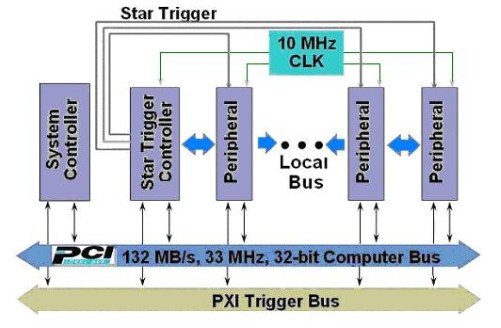
- 10 MHz Backplane Clock: Consists of a 10 MHz clock signal routed to all PXI slots but Slot 1 (the controller slot) through equal-length traces. The PXI Specification specifies that this signal must have an accuracy of at least +/- 100 ppm. NI chassis offer an accuracy of +/- 25 ppm. It can be overridden by another 10 MHz clock sourced by a capable PXI module installed in Slot 2 or by a CLK10 signal coming from another chassis (i.e. PXI-1042). Some PXI boards normally use the CLK10 signal as the reference signal to synchronize their internal clocks using Phase-Lock Loop (PLL) techniques.
- PXI Star Trigger: Can be driven by a module installed in Slot 2 with PXI Star Trigger capabilities. A digital TTL signal can be sent from slot 2 to the 13 slots to its right, through equal-length traces. The result is a propagation delay of no more than 5 ns, so the signal will arrive to all slots practically at the same time. It is very useful for applications where different PXI boards need to start a process at the same time. The PXI Star Trigger line has been tested with TTL signals up to 105MHz.
- PXI Trigger Bus: A bus of eight lines over which all PXI slots, including the controller slot, can send and receive timing and triggering digital TTL signals. To preserve the quality of the signal, sending TTL digital signals with frequencies above 20 MHz is not recommended.
- Local Bus: Each peripheral slot has two buses of 13 lines that connect it to the adjacent modules to its right and to its left. These local bus lines are capable of passing high-speed digital and analog signals (up to 42 V).
NOTE: Slot 2 only has a local bus to its right because the left local bus is replaced with the Star Trigger.
All PXI chassis will make the features listed above available to the appropriate slots. It is up to the designer of the PXI board to route signals to the pins in the PXI backplane to take advantage of these features. Therefore, not all PXI boards will be able to use all of the timing and synchronization features available on the PXI backplane. Driver documentation and manual for your specific board should explain what features of the PXI backplane your board is capable of using.
What are the requirements for my PXI board to use the PXI Timing and Synchronization features in the PXI backplane?
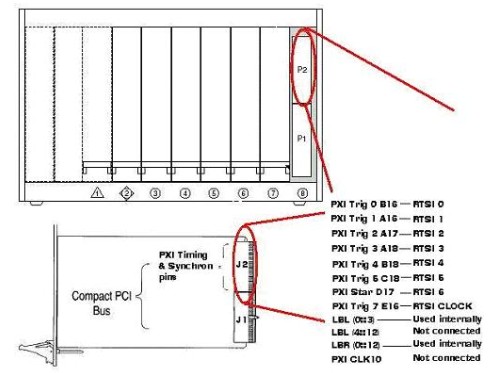
- The PXI board needs to have physical hardware connections to the pins in the PXI backplane that correspond to the different timing and synchronization features. The User Manuals for the NI boards either describe verbally or show in a table, how signals in the board map to pins on the backplane. The table below corresponds to Table 1-1 in the PXI E Series User Manual. It shows how signals in these boards map to pins in the PXI backplane:
| PXI E Series Signal | PXI Pin Name | PXI J2 Pin Number |
|---|---|---|
| RTSI Trigger (0...5) | PXI Trigger (0..5) | B16,A16,A17,A18,B18,C18 |
| RTSI Trigger (6) | PXI Star | D17 |
| RTSI Clock | PXI Trigger (7) | E16 |
| Reserved | LBL(0..3) | C20, E20, A19, C19 |
| Reserved | LBR(0..12) | A21, C21, D21, E21, A20, B20, E15, A3, C3, D3, E3, A2, B2 |
This means that the PXI E series boards use PXI Trigger Lines 0,1,2,3,4,5,7, but not PXI Trigger Line 6. They are capable of reading the PXI Star Trigger Line and they cannot read the PXI Backplane Clock. The board has physical connections to some of the Local Bus Left lines (0 through 3) and to all the Local Bus Right lines. However, these lines are reserved by the driver, that is, NI-DAQ does not provide any function that allows the user to have access to these lines. With the NI-DAQmx driver, you can unreserve these lines in NI MAX under your chassis configuration. See the image below for a graphical representation of the table.
- If the PXI board is capable of performing different functions, depending on the slot that the board is installed in, the driver needs to be able to configure the board accordingly. This means that even if the board has physical connections to the timing and synchronization pins in the PXI backplane, it is up to the programmer of the driver to implement the functions that will allow the user to use those connections. NI drivers allow you to take advantage of the capabilities of your PXI boards.
- The last requirement is to save the appropriate PXI System Initialization file (PXISYS.INI) in the Systems directory of your computer. The PXISYS.INI file describes the architecture of the system and pairs up the PCI slot in the PXI chassis with the Slot number printed in the front of the chassis.
Note: MAX 3.x can automatically generate the correct PXISYS.INI file and place it in the correct location. For instructions on configuring your PXI system in Legacy Versions of MAX and information about PXISYS.INI, please refer to the Configuring Your PXI system in Legacy Versions of MAX. The PXI Specification defines 3 different types of slots in a PXI chassis:
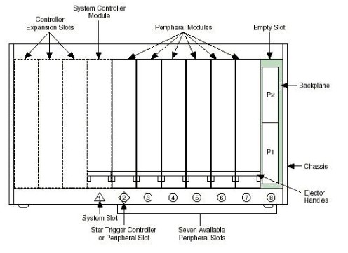
- System slot: always the left most slot of the chassis. It is numbered Slot number one and its glyph is a triangle. In this slot you install the controller of the system.
- Star Trigger controller: the second slot in the PXI chassis. To drive the PXI Star Trigger line you need to install a PXI board that is capable of driving this line in Slot 2. To override the CLK10 you need to install a PXI board capable of overriding the CLK10 signal in Slot 2. Its glyph is a square, rotated by 45º. You can also install normal PXI boards with no special capabilities in this slot. That is, you can also use this slot as a peripheral slot. That is why the glyph also includes the same glyph for peripheral modules (see image below)
- Peripheral slot: all slots in the chassis other than Slot 1 and 2. Install in these slots any PXI/CompactPCI boards. Some PXI boards are capable of reading the PXI Star Trigger, CLK10 signals or PXI Trigger Lines. Some others are capable of using the Local Buses to share data with adjacent modules. As explained earlier, access to these different timing and synchronization features will depend on how the PXI board was designed.
The image below shows the type of slots of a NI PXI-1042 chassis with their numeration and glyphs:
It is necessary to save the PXISYS.INI file in the Systems directory in your computer so drivers can find it and read it. This way a driver can find out in what slot of the PXI chassis the board is installed. The drivers then will enable different circuits on the board depending on the slot that the board is located.
For example, a PXI-6608 counter board is capable of overriding the CLK10 signal in the PXI backplane. However the board will not override the CLK10 signal automatically. First the driver of the board, in this case NI-DAQ or NI-DAQmx, needs to read the PXISYS.INI file to find out if the board is installed in slot 2 of the PXI chassis. If this is correct, then the driver sends the appropriate commands to the PXI-6608 board to route the internal CLK10 signal to the PXI CLK10 signal.
How does my NI PXI board use the PXI backplane?
| Available PXI BoardFunctions | NI PXI Boards | Additional Comments |
|---|---|---|
| Override the CLK10 signal |
|
|
| Phase Lock Loop (PLL) to the CLK10 signal |
|
|
| Drive the PXI Star Trigger |
|
|
| Receive the PXI Star Trigger |
|
|
| Read and Write to PXI Trigger Lines | Most NI PXI boards can read and write to the PXI Trigger lines | These PXI boards have 7 RTSI internal lines that are routed to the pins in the PXI backplane in the following way:
|
| Use Local Bus |
| The only NI PXI boards that use the Local Bus are the ones that can control the SCXI portion of PXI Combo chassis (PXI-101x chassis) when installed in the right most slot of these chassis. The following are some of the capabilities of each type of board:
|


