NI does not actively maintain this document.
This content provides support for older products and technology, so you may notice outdated links or obsolete information about operating systems or other relevant products.
When configuring the USRP RIO Reference Clock, the NI-USRP driver included in LabVIEW Communications System Design Suite, also referred to as LabVIEW Communications, version 1.1 stops several hardware clocks during reconfiguration. Accessing any configuration registers during that time creates an FPGA access violation. In the host implementation of the LTE Application Framework version 1.0, the Reference Clock was configured during runtime, which causes this access violation.
The implication of the FPGA access violation are as follows:

Figure 1 - Error message -61046
You can avoid the FPGA access violation by not reconfiguring the Reference Clock source during runtime. The remainder of this document describes the necessary code changes. These instructions apply for designs that are based on the LTE Application Framework version 1.0 and consists of two parts:
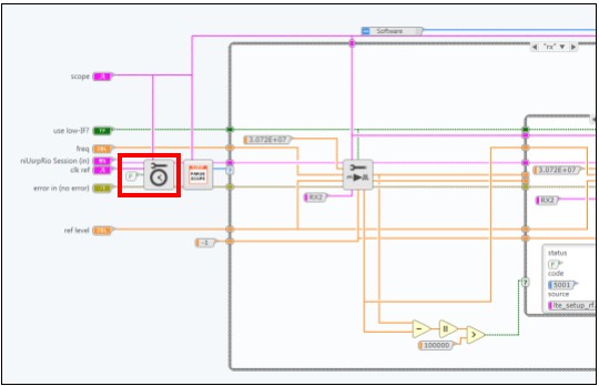
Figure 2. lte_setup_rf.gvi (Unmodified)
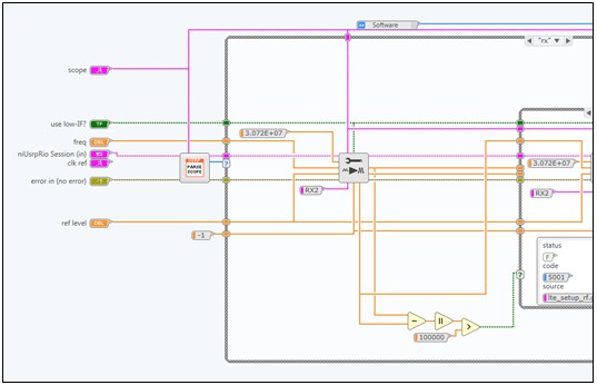
Figure 3. lte_setup_rf.gvi (Modified)
This part of the code change is only required if you want to use another clock source as the internal clock.
Figure 4. lte_host_init.gvi (Unmodified)
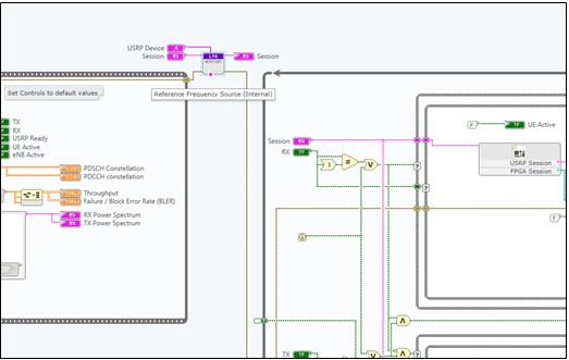
Figure 5. lte_host_init.gvi (Modified)
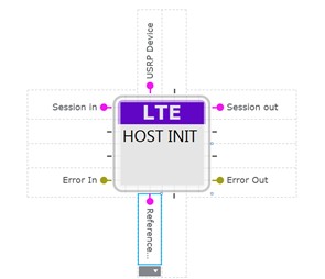
Figure 6. Icon Pane of lte_host_init.gvi
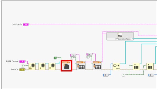
Figure 7. lte_host_usrp_rio.gvi (Unmodified)

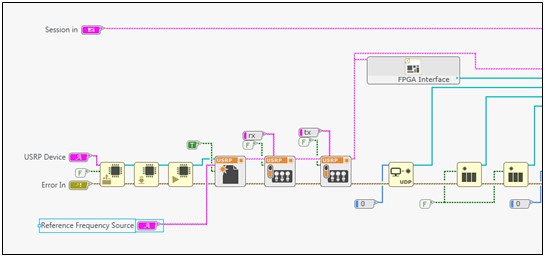
Figure 8. lte_host_usrp_rio.gvi (Modified)
Figure 9. lte_host_usrp_rio.gvi Panel
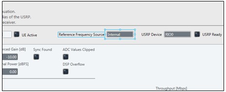
Now this control sets the reference frequency source for the USRP RIO. Valid values:
Changing the reference frequency source requires you to restart the application. The former controls TX Reference Clock and RX Reference Clock now do not function. They may be removed from the panel.