LabVIEW Communications LTE Application Framework 1.1 White Paper
Overview
The LTE Application Framework provides a ready to run, easily modifiable real-time physical layer (PHY) and lower medium access control (MAC)-layer reference design based on the LTE wireless standard. The LTE Application Framework is available with the LabVIEW Communications System Design Suite, also referred to as LabVIEW Communications.
Contents
Intro
This application framework provides a substantial starting point for researchers looking for ways to improve the LTE standard by exploring brand-new algorithms and architectures that can support the tremendous increase of the number of terminals, inventing new waveforms by which to modulate and demodulate the signals, or finding new multi-antenna architectures that fully exploit the degrees of freedom in the wireless medium.
The LTE application framework is comprised of modular PHY and MAC blocks implemented using LabVIEW Communications. It is designed to run on the powerful Xilinx Kintex-7 FPGA and an Intel x64 general purpose processor, which are tightly integrated with the RF and analog front ends of the NI software-defined radio (SDR) hardware.
The framework is designed from the ground up for easy modifiability, while adhering to the main specifications of the LTE standard. This design allows wireless researchers to quickly get their real-time prototyping laboratory set up and running based on the LTE standard. They can then primarily focus on selected aspects of the protocol that they wish to improve, and easily modify the design and compare their innovations with the existing standards.
Scope
The LTE Application Framework provides the functional elements of the physical (PHY) layer as well as medium access control (MAC) layer of both base station (eNodeB) and user equipment (UE). This code includes the following elements:
- Downlink transmission (DL TX) and reception (DL RX)
- Uplink transmission (UL TX) and reception (UL RX)
Additionally, basic MAC functionalities are provided that allow for the following features:
- Packet-based user data transmission in downlink, enabling user data-streaming applications
- Feedback of DL channel state information and DL (HARQ) ACK/NACK through the uplink
- Basic adaptive modulation and coding (AMC), which includes link adaptation in downlink, enabling DL closed loop operations
The following subsections describe in more detail which principal operation modes are provided by the LTE Application Framework and which specific subset of PHY and MAC functionalities of a 3GPP LTE release 10 compliant system is implemented.
Deviations and simplifications with respect to the 3GPP LTE releases 10 standard are also described here. They have been applied to keep the complexity of the Application Framework at a reasonable level.
2.1 Operation Modes
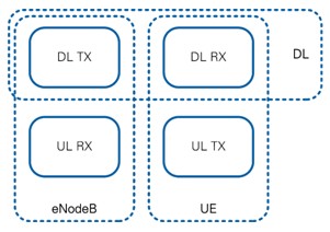
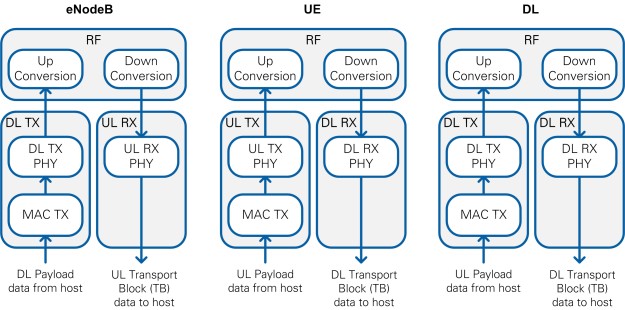
The LTE Application Framework offers three operation modes, as depicted in Figure 1. These three operation modes are provided by the following pairs of top-level host and top-level FPGA implementations:
- Downlink (DL):
- Can be used to establish a downlink link in either a single-device setup or a double-device setup.
- Implements the downlink transmitter (DL TX) of a base station (eNodeB) and the downlink receiver (DL RX) of a user equipment (UE) including the basic DL TX and DL RX MAC functionalities
- In a single-device setup, a special “MAC shortcut” (refer to Figure 12 in section 3.1) allows for downlink AMC (rate adaptation) even without a real uplink feedback channel
- Top-level host VI: LTE Host DL.gvi
- Top-level FPGA VI is one of the following VIs:
- LTE FPGA FlexRIO DL.gvi
- LTE FPGA USRP RIO 40 MHz BW DL.gvi
- LTE FPGA USRP RIO 120 MHz BW DL.gvi
- eNodeB:
- Provides the base station (eNodeB) side in a double-device setup.
- Implements the downlink transmitter (DL TX) and the uplink receiver (UL RX) of an eNodeB including the basic eNB MAC functionalities (see upper part of Figure 13)
- Top-level host VI: LTE Host eNodeB.gvi
- Top-level FPGA VI is one of the following VIs:
- LTE FPGA FlexRIO eNodeB.gvi
- LTE FPGA USRP RIO 40 MHz BW eNodeB.gvi
- LTE FPGA USRP RIO 120 MHz BW eNodeB.gvi
- UE:
- Provides the user equipment (UE) side in a double-device setup
- Implements the downlink receiver (DL RX) and the uplink transmitter (UL TX) of a UE including the basic UE MAC functionalities (see lower part of Figure 13)
- Top-level host VI: LTE Host UE.gvi
- Top-level FPGA VI is one of the following VIs:
- LTE FPGA FlexRIO UE.gvi
- LTE FPGA USRP RIO 40 MHz BW UE.gvi
- LTE FPGA USRP RIO 120 MHz BW UE.gvi
Figure 1: System Configurations (Host and Associated FPGA Code)
The downlink (DL) operation mode can be used either in a single-device setup or in a double-device setup. The eNodeB/UE operation modes require a double-device setup.
2.2. Physical Layer (PHY)
The LTE application framework implements parts of a 3GPP-LTE release 10 compliant downlink and uplink physical layer transmitter and receiver. To keep the complexity of this application framework at a reasonably low level, only a subset of the physical layer features defined for 3GPP-LTE release 10 compliant devices is implemented. This subset also includes feature simplifications and limitations of the configurability of the implemented PHY features, for example, specific configuration parameters are fixed to single values, and others are only quasi-statically configurable. Notice that fixed parameter settings can only be changed by modifying the design.
The following subsections give a detailed overview over the implemented PHY features, used simplifications, and (potentially restricted) PHY configuration capabilities with respect to the 3GPP LTE releases 10 specifications.
2.2.1. Frame Structure, Bandwidth Mode, CP Mode, and Physical Resource Grid
The LTE Application framework supports the following (partially fixed) configurations:
- Bandwidth mode: 20 MHz (100 PRBs)
- Cyclic prefix configuration: Normal cyclic prefix
- Frame Structure:
- Type 1—FDD
- Type 2—TDD
- TDD uplink-downlink configuration: 5
- Special subframe configuration: 5
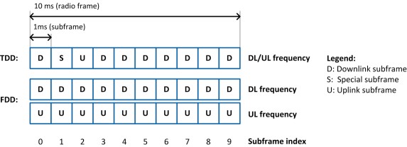
The detailed radio frame structure for both frame structure types is shown in Figure 2. Each radio frame is 10 ms long and consists of 10 subframes. Each subframe has a length of 1 ms, which comprises 30,720 complex time-domain baseband samples sampled at a rate of 30.72 MS/s, which is valid for the 20 MHz LTE bandwidth mode. The related sample period Ts is (1/30.72e6) s. The types of subframes vary with the subframe index in dependence on the selected radio frame type. Downlink subframes (D) are reserved for downlink transmissions; uplink subframes (U) are reserved for uplink transmissions. Special subframes (S) are used with frame structure type 2 (TDD) only. For TDD uplink-downlink configuration 5, which is supported by the LTE application framework, there is only one special subframe per radio frame. Special subframes consists of the following fields:
- DwPTS – Downlink pilot time slot
- Reserved for downlink transmission
- In the LTE Application Framework, it is restricted to transmission of Physical downlink control channel (PDCCH) and cell-specific reference signals (CRS)
- Length: fixed to 3 OFDM symbols (6,592 * Ts)
- GP – Guard Period
- Time-domain guard period for switching between active downlink transmission/reception and active uplink reception/transmission
- Length: fixed to 9 OFDM symbols (19,744 * Ts)
- UpPTS – Uplink pilot time slot
- Reserved for transmission of uplink sounding reference symbols (SRS)
- Length: fixed to 2 OFDM symbols (4,384 * Ts)
According to [1], the length of the special subframe fields varies with the special subframe configuration and the selected cyclic prefix configuration. In the current LTE Application Framework, implementation of both parameters are fixed to specific settings, so the special subframe fields have a fixed length.
Figure 2: Subframe types for TDD and FDD Frame Structure
For normal cyclic prefix configuration, each subframe is divided into 14 OFDM symbols. The OFDM symbol duration is 2,048 * Ts extended by a cyclic prefix of 160 * Ts for OFDM symbols 0 and 7 and a cyclic prefix of 144 * Ts for all other OFDM symbols in a subframe.
For the 20 MHz LTE bandwidth mode, a 2,048-point IFFT is specified to be used in the OFDM modulator, in other words, 2,048 frequency-domain subcarriers per OFDM symbol are available. According to [1], only the inner 1,200 subcarriers, excluding the DC carrier, are allowed to be used for actual signal transmissions. The remaining unused subcarriers act as a guard band for neighboring channels. The set of 1,200 usable subcarriers, also called resource elements, are organized in sets of 12 contiguous subcarriers corresponding to the physical resource blocks (PRBs). Notice that one PRB comprises the same set of 12 contiguous subcarriers, or resource elements, of multiple consecutive OFDM symbols, such as all OFDM symbols of a slot or subframe. For further details see [1].
2.2.2. Physical Downlink Channels and Signals
2.2.2.1. Overview
The downlink transmitter and receiver each include FPGA implementations of the following channels:
- Primary Synchronization Signal (PSS)
- Cell-Specific Reference Signals (CRS)
- UE-Specific Reference Signals (UERS)
- Physical Downlink Control Channel (PDCCH)
- Physical Downlink Shared Channel (PDSCH)
The following downlink channels and signals are not implemented:
- Secondary Synchronization Signal (SSS)
- MBSFN reference signals
- Positioning reference signals
- CSI reference signals
- Physical Control Format Indicator Channel (PHICH)
- Physical Hybrid-ARQ Indicator Channel (PCFICH)
- Physical Broadcast Channel (PBCH)
- Physical Multicast Channel (PMCH)
The supported physical channels and signals are in general implemented in compliance with 3GPP LTE release 10 specifications [1], [2], [3]. Any specific deviations, extensions, simplifications, or configuration restrictions are explained in the corresponding sub-sections below.
A general restriction, which holds for all channels and signals if not mentioned otherwise, is that the Cell-ID is fixed to 0.
2.2.2.2. Primary Synchronization Signal (PSS)
The PSS is transmitted only once per radio frame, with a periodicity of 10 ms instead of a periodicity of 5 ms. This adaption to the LTE specification is necessary to realize a unique detection of the radio frame start without SSS support. Depending on the selected frame structure type the PSS is transmitted in one of the following ways:
- The third OFDM symbol of subframe 1 for TDD
- The seventh OFDM symbol of subframe 0 for FDD
The PSS sequence generation is implemented for Cell-ID 0 only.
2.2.2.3. Cell-Specific Reference Signals (CRS)
CRS resource elements are always reserved (allocated) for two antenna ports. Active CRS transmissions are done on the first antenna port only.
Sequence generation as well as resource mapping (cell-specific frequency shift) are implemented for the fixed Cell-ID 0 only.
2.2.2.4. UE-Specific Reference Signals (UERS)
UE-specific reference signals (UERS) can be optionally enabled in additional to CRS. The following features and configurations are supported:
- Supported on antenna ports 7 to 14; not supported on antenna port 5
- Supported in downlink subframes only; not supported in special subframes
- Sequence generation as specified in [1] for antenna ports 7 to 14
- Implemented for fixed Cell-ID and parameter fixed to 0
- With UERS support enabled the resource elements for both UERS antenna port sets {AP 7, 8, 11, 12} and {AP 9, 10, 13, 14} are reserved in each slot of a downlink subframe while active UERS transmission and reception is only performed for the selected antenna port. Notice that this is a deviation from (an extension to) the 3GPP LTE specification [1] and would be a prerequisite for TM9, like multiuser MIMO for up to 8 UEs.
If UERS are enabled, UERS-based channel estimates, instead of CRS-based channel estimates, are used by the downlink receiver to equalize the PDSCH.
Note: The UERS based channel estimation in the downlink receiver applies a simple interference cancellation scheme to reduce interference potentially caused by simultaneous code-orthogonal UERS transmissions on the same UERS resource elements. The underlying cancellation algorithm, which cannot be disabled in the current implementation, is designed for slowly time-varying radio channels only, which means that assumes the radio channel to be sufficiently time-invariant over a time period of one subframe (1ms).
2.2.2.5. Physical Downlink Control Channel (PDCCH)
The PDCCH implemented in the LTE application framework mainly follows the specifications in [1], [2], [3], but is partially simplified and therefore is partially proprietary.
2.2.2.5.1. PDCCH Resource Grid
The LTE application framework supports the PDCCH to be transmitted only in the first OFDM symbol of each downlink or special subframe. This corresponds to a fixed control format indicator (CFI) of 1. All available (non-CRS occupied or reserved) resources are used for PDCCH as PCFICH and PHICH are not part of the implementation.
2.2.2.5.2. PDCCH Format
The LTE standard allows for several different PDCCH formats (refer to [1] section 6.8.1), which differ in the so-called aggregation level, such as the number of consecutive control channel elements (CCEs) used for transmitting one downlink control information (DCI) message on the PDCCH. One CCE comprises nine resource element groups (REGs) with four resource elements (RE) per REG. Since the PDCCH is specified to use QPSK modulation, 2 bits per RE can be transmitted which finally comes to 72 bits per CCE.
The PDCCH format implemented in the LTE application framework is fixed to format 1, which corresponds to a fixed aggregation level of 2. Thus, always 2 consecutive CCEs are used for transmitting one DCI message. This format corresponds to the allocation of 18 REGs (72 REs), which allows for the transmission of 144 encoded bits per DCI message.
2.2.2.5.3. DCI Format
The implemented downlink control information (DCI) format is partially proprietary. It corresponds to a subset of the LTE DCI Format 1. As illustrated in Figure 3, it consists of the following three fields:
- PRB allocation—Used for signaling the PRB allocation for the PDSCH.
- MCS—Used for signaling the PDSCH modulation and coding scheme.
- TPC—Reserved for actions such as the uplink transmit power control commands, currently not used.
Each bit of the PRB Allocation field represents 4 PRBs (according to DL resource allocation type 0, see [3] section 7.1.6.1). The leftmost bit represents the lowest resource block (group) index. The MCS signaling is compliant with the LTE standard, see [3] section 7.1.7. The supported MCS value range is restricted to 0...28. MCS 29, 30 and 31 are not supported as there is no HARQ processing included.
Figure 3: PDCCH DCI Format
Note: With the described DCI format only DL scheduling grants can be signalized using the PDCCH while uplink scheduling information are not supported to be sent with PDCCH. Thus, the uplink transmitter at the UE, as well as the uplink receiver at the eNB, must be configured manually using the respective host application.
The overall number of bits used for the supported DCI format is 32.
2.2.2.5.4. DCI Encoding
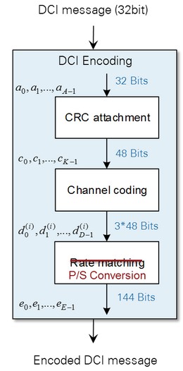
The DCI encoding mainly follows the 3GPP LTE release 10 specification. CRC attachment and channel coding are fully compliant with [2], but the rate matching is substituted by a simple parallel-to-serial conversion as is shown in Figure 4. According to [2], the LTE rate-matching block requires a subblock interleaver per parity bit output stream of the convolutional channel encoder, followed by a bit collection stage and a circular buffer, which is used for the actual rate adaptation (such as for bit puncturing (pruning) or repetition).
For the combination of the fixed PDCCH format (refer to section 2.2.2.5.2) and the fixed modified DCI format (refer to section 2.2.2.5.3) implemented by the LTE application framework, there is no need for any rate adaptation. The number of output bits delivered by the 1/3-rate convolutional channel encoder exactly matches with the number of bits that can be transmitted by the supported PDCCH format 1 (2 CCEs produces 144 bits). Thus, in this case the rate matching can be skipped.
Note: For reasons of simplicity the parallel-to-serial conversion implemented in the LTE Application Framework instead of the rate matching collects the parity output bits of the convolutional encoder as follows:
d0(0), d0(1), d0(2), d1(0), d1(1), d1(2), ...
This equation is different than the way the bit collection stage is defined for the LTE-compliant rate matching. This stage collects the bits as follows:
where v(i) stands for the interleaved version of ith parity bit output d(i) stream of the channel encoder.
Figure 4: Modified DCI Encoding Scheme
2.2.2.5.5. PDCCH Multiplexing, Scrambling, Modulation, and Resource Mapping
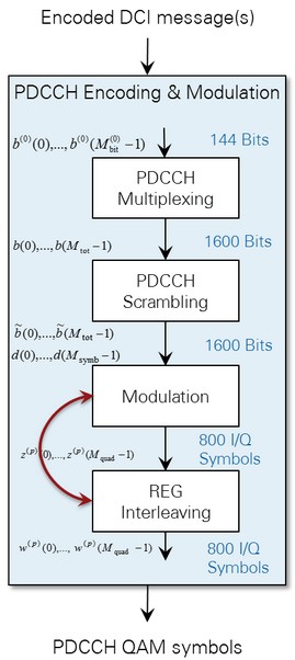
Figure 5 shows the further PDCCH processing with the following functionalities:
- PDCCH multiplexing
- Scrambling
- Modulation
- Layer mapping and precoding
- Mapping to resource elements
It is implemented in compliance with the specifications in [1] with the following simplifications:
- PDCCH multiplexing currently supports only 1 control channel (DCI message) to be transmitted per subframe.
- There are eight possible CCE positions, which are pairs of consecutive CCEs that can be manually selected using the CCE offset parameter. This is a prerequisite for multi-user support for up to 8 UEs.
- No support of automatic CCE selection (PDCCH assignment) in dependence on RNTI and search space (as defined in [3] section 9.1.1).
- QPSK modulation as specified in [1], but for reasons of implementation efficiency modulation is performed after the REG interleaving.
- Note: This specific implementation does not influence the final output of the overall PDCCH processing.
- Layer mapping and precoding are supported for transmission on a single antenna port (transmission mode 1) only.
- Since this is a one-to-one mapping, the block does not need to be implemented at all.
- REG interleaving supported for fixed Cell-ID value 0 only
- For this Cell-ID value the cell-specific cyclic shift, which is specified in [1] in addition to the actual interleaver functionality, becomes transparent and therefore is not implemented.
Figure 5: PDCCH Processing
2.2.2.6. Physical Downlink Shared Channel (PDSCH)
Channel coding, scrambling, and modulation of the PDSCH are implemented in the LTE application framework in compliance with [1], [2] with the following restriction:
- HARQ support is not implemented.
Layer mapping and precoding are implemented for transmission on single antenna port (transmission mode 1) only.
The PDSCH resource mapping is compliant with [1] with the following exceptions:
- PDSCH transmission is supported in downlink subframes only; not supported in special subframes.
- The PDSCH resource mapping is adapted to the modified or restricted resource mapping of PSS, CRS, and UERS.
- Resource elements outside the PDCCH region available from channels and signals which are not implemented (e.g. SSS, PBCH) are used for PDSCH.
- For activated UERS PDSCH is not transmitted in resource blocks in which parts of the UERS (due to potential overlap with other PHY channels or signals) are not transmitted.
- This restriction currently applies for frame structure type 1 (FDD) where the PRBs centered around DC in subframe 0 are not used for PDSCH transmissions due to the potential overlap with the PSS.
- To ease the handling for the user the related conditions will be automatically checked by the FPGA implementation of the downlink transmitter and the PDSCH resource allocation will be automatically modified for the affected subframes. The modified PDSCH resource allocation will be applied for the whole PDSCH processing (including the transport block size determination) as well as for the related DCI content signaled on the PDCCH. As the currently implemented DCI format only allows for signaling the allocation of 4 consecutive PRBs, not only the 6 PRBs colliding with PSS but in total the 12 innermost PRBs will not be used for PDSCH transmission in this special case.
The LTE application framework supports a quasi-static PDSCH resource allocation at the downlink transmitter using resource allocation type 0 according to [3]. Thus, for the supported 20MHz bandwidth mode 25 resource block groups (RBGs) can be individually allocated. Each RBG addresses a set of 4 consecutive PRBs.
The PDSCH modulation order and transport block size determination follows the specifications in [3] tables 7.1.7.1-1 and 7.1.7.2.1-1. They can be controlled at the downlink transmitter by means of the modulation and coding scheme (MCS) parameter. The LTE application frameworks supports all MCS between 0 and 28. MCS 29…31, which are only applicable with full DL HARQ support, are not implemented. For activated UERS MCS 28 is not supported since the resulting code rate would exceed 1 due to the modified UERS mapping.
Note: The selected PDSCH resource allocation as well as the selected modulation and coding scheme (MCS) are signaled to the downlink receiver via the PDCCH. Thus, the PDSCH configuration is applied automatically in the receiver and does not need to be set manually.
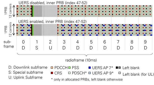
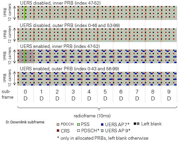
2.2.2.7. Supported DL Resource Grid
Figure 6 shows the resulting LTE downlink resource grid for frame structure type 2 (TDD) with all supported physical downlink channels and signals. It exemplarily shows the resource grid for the inner PRBs centered around DC which contain PSS. The resource mapping in the outer PRBs is in principle the same with the only difference that they do not contain PSS, instead the corresponding resource elements are left blank.
Figure 7 shows the resulting LTE downlink resource grid for frame structure type 1 (FDD) with all supported physical downlink channels and signals. The resource grid for both kind of PRBs, i.e. inner PRBs (containing PSS and PSS reserved REs) and outer PRBs (not containing PSS) are shown.
Figure 6: Supported LTE DL Resource Grid for Frame Structure Type 2 (TDD)
Figure 7: Supported LTE DL Resource Grid for Frame Structure Type 1 (FDD)
2.2.3. Physical Uplink Channels and Signals
2.2.3.1. Overview
The uplink implementation in the LTE application framework is using OFDMA instead of SC-FDMA. Neither the PUSCH DFT spreading nor the LTE uplink specific half subcarrier shift are applied. Simple OFDM modulation is used instead with a zero DC subcarrier inserted, similar to the LTE downlink specification.
The uplink transmitter and receiver implementations comprise the following physical channels and signals:
- Physical uplink shared channel (PUSCH)
- Demodulation reference signals (DMRS)
- Sounding reference signal (SRS)
The following uplink channels and signals are not available:
- Physical random access channel (PRACH)
- Physical uplink control channel (PUCCH)
2.2.3.2. Physical Uplink Shared Channel (PUSCH)
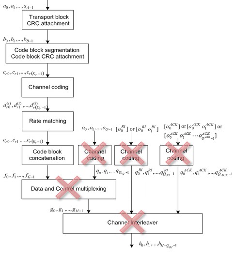
The PUSCH implemented in the LTE application framework applies a slightly simplified coding scheme in comparison to the specifications in [2]. The applied simplifications are illustrated in Figure 8. The resulting coding scheme is very similar to the coding scheme used for PDSCH. The specifics in comparison to full standard compliant PUSCH encoding are the following:
- Only the coding for the Uplink Shared Channel (UL-SCH) data is supported.
- Coding and multiplexing of Uplink Control Information (UCI) on PUSCH is not supported.
Figure 8: Simplified UL-SCH Coding Scheme
PUSCH scrambling, modulation, layer mapping, and pre-coding are implemented in compliance with [1] with the following restriction:
- Layer mapping and precoding are implemented for transmission on single antenna port only.
The PUSCH transform precoding (DFT spreading) specified in [1] sec. 5.3.3 is not implemented since the LTE applications framework applies OFDM instead of SC-FDMA in the uplink.
The supported PUSCH resource mapping is compliant with the specifications in [1] with the following restriction:
- For activated SRS support the last OFDM symbol cannot be used for PUSCH at all, even if the UE is not actively transmitting SRS.
- PUSCH transmission are only allowed on contiguous resource block sets.
- Uplink frequency hopping (PUSCH hopping) is not implemented.
The LTE application framework supports a quasi-static PUSCH resource allocation at the uplink transmitter and uplink receiver using resource allocation type 0 according to [3]. Similar to the PDSCH allocation in the downlink 25 resource block groups (RBGs) can be individually allocated for PUSCH in uplink. Each RBG addresses a set of 4 consecutive PUSCH PRBs.
In the LTE application framework the PUSCH modulation order and transport block size determination uses the same MCS tables (see [3] Tables 7.1.7.1-1 and 7.1.7.2.11) as applied for the PDSCH. This is a slight deviation from the LTE standard which originally defines a slightly different MCS scheme for the PUSCH. The MCS can be quasi-statically selected at the uplink transmitter and receiver in the range between 0 and 28.
Note: Since no uplink scheduling information is signaled from eNB to UE via the PDCCH, PUSCH resource allocation as well as PUSCH MCS have to be manually configured at both devices.
2.2.3.3. Demodulation Reference Signals (DMRS)
According to the LTE standard, DMRS are associated with the transmission of PUSCH or PUCCH. Since the LTE application framework does not provide a PUCCH implementation, only DMRS associated with PUSCH are supported. For the supported frame structure and the supported normal CP mode, DMRS are transmitted in the fourth and the 11th OFDM symbol of an uplink subframe, but only in those PRBs that carry PUSCH (refer to Figure 9).
The DMRS sequence generation implemented in the LTE application framework is slightly simplified in comparison to the specification in [1]. In deviation to the LTE standard, DMRS sequences of different lengths (required for different numbers of allocated PUSCH PRBs) are all derived from one fixed base sequence defined for 100 PUSCH PRBs (i.e. for the maximum supported number of PUSCH PRBs). Shorter DMRS sequences are derived by taking the maximum length base sequence and cutting surplus symbols at the end. The base sequence generation itself is compliant with Sections 5.5.1 and 5.5.1.1 of [1]. The following fixed parameter set is applied for the base sequence generation.
Since the sequence-group number u as well as the base sequence number v are both fixed to 0, this implies that neither group hopping nor sequence hopping are supported.
2.2.3.4. Sounding Reference Signal (SRS)
In the LTE application framework, uplink SRS support can be globally enabled or disabled. When SRS support is enabled, the last OFDM symbol in every UL subframe is reserved for SRS transmissions, so it cannot be used for any other UL signal or channels anymore. This statement is true even if the uplink transmitter is not actively transmitting SRS in the corresponding uplink subframes. In TDD mode (frame structure type 2), the last 2 symbols of a special subframe can be used for SRS transmissions.
Active SRS transmissions can be individually scheduled for every UL subframe and every special subframe per radio frame. According to [1] section 5.5.3.3, this scheduling corresponds to the following positions:
- srs - SubframeConfig = 0 for FDD
- srs - SubframeConfig = 7 for TDD in general
(which is also equivalent to srs - SubframeConfig = 1 for TDD5/5) - For this purpose a special parameter is provided at the control interfaces of the uplink transmitter and receiver. It is a bit vector with 10 elements, and each element addresses one specific subframe of a radio frame. In TDD mode, this bit vector is masked with the supported pattern of special and uplink subframes to ensure that active SRS transmissions are only possible in these subframes. For individually addressing the 2 SRS symbols in the UpPTS field of a special subframe, the following rule is applied in TDD mode:
- The bit related to a special subframe controls SRS transmissions in the last OFDM symbol of the special subframe.
- The bit related to the DL subframe preceding a special subframe controls SRS transmission in the previous last OFDM symbol of that special subframe.
The SRS bandwidth used is always fixed to 96 PRBs, which corresponds to SRS bandwidth configuration C_SRS = 0 and SRS bandwidth B_SRS = 0.
The SRS transmission comb k_TC can be directly configured to be 0 or 1. SRS frequency hopping is not supported.
The SRS sequence generation is implemented in compliance with [1] section 5.5.3.1 and 5.5.1, but only the following fixed parameter set is supported.
As explained in section 2.2.3.3 for the DMRS, this implies that neither group hopping nor sequence hopping are supported.
The SRS transmitter is fully implemented. On the receiver side the SRS subcarrier data are extracted, but currently no further receiver operation is implemented.
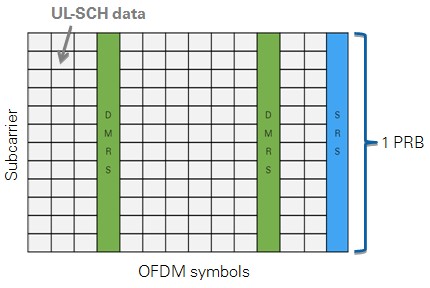
2.2.3.5. Supported UL Resource Grid
Figure 9 shows exemplarily the supported resource grid for an uplink subframe with active SRS.
Figure 9: Time-Frequency Resource Grid of an Uplink Subframe with Enabled SRS Support
2.2.3.6. Uplink Transmit Timing Control
You can control the uplink transmit timing at the UE transmitter in a quasi-static manner using the uplink timing advance parameter. In the LTE Application Framework, the uplink timing advance is set to zero per default. Zero means that the start of the transmitted uplink radio frame is fully aligned to the start of the received downlink radio frame at the UE antenna connectors. To cope with the propagation delay of real radio channels, the start of the uplink can be advanced by 0 up to 30,719 baseband samples, such as by 0 through 30,719 * Ts with Ts = 1/(30.72 MHz).
Note: [1] defines a fixed timing advance offset NTAoffset = 624xTs for frame structure type 2 (TDD). This offset is not automatically applied by the LTE application frame in TDD mode, but has to be set manually if needed.
In addition to the uplink timing advance mechanism, the LTE application framework autonomously corrects the UL transmit timing in relation to the downlink radio frame timing measured at the UE receiver. Thus, time tracking steps applied in the downlink receiver are also applied to the uplink transmitter. The time tracking is designed to cope with clock frequency differences between eNB and UE of up to ±5 ppm. Potential timing corrections are applied once per radio frame at the beginning of the radio frame.
They are realized by reducing or extending the cyclic prefix by an integer number of baseband samples. The current implementation allows for maximum correction steps of up to ±160 baseband samples (±160 * Ts). As long as the observed clock frequency difference is below the target maximum of ±5 ppm, the maximally applied timing correction step should be below ±2 * Ts, which is the upper limit defined by the LTE standard.
2.2.3.7. Uplink Frequency Offset Correction
In addition to the autonomous UL transmit timing correction, the LTE application framework also applies an autonomous UL frequency offset correction. Carrier frequency offsets measured and corrected in the downlink receiver are also applied in the uplink transmitter with a carrier frequency depending scaling factor -1 * fC,UL/fC, DL. Notice that frequency shifts in the uplink transmitter must be applied in the opposite direction as in the downlink receiver. For FDD, the ratio between uplink carrier frequency and downlink carrier frequency must be taken into account.
2.3. Medium Access Control Layer (MAC)
The LTE Application Framework implements the necessary functionality for establishing a link between the eNB (DL transmitter) and UE (DL receiver) and for enabling packet-based data transmission in the downlink. Furthermore it provides the following features:
- Feedback of DL channel state information and DL (HARQ) ACK/NACK via the uplink
- Basic adaptive modulation and coding (AMC), known as link adaptation in downlink, enabling DL closed loop operations
2.3.1. System Configuration
The system configuration is fixed to the following values at both the Downlink Transmitter (eNodeB) and Downlink Receiver (UE):
- Bandwidth: 20 MHZ (100 PRBs)
- Cell-ID: 0
- Control Format = 1 (PDCCH spans over one OFDM symbol per subframe)
- Antenna configuration: single antenna (SISO)
Because of the fixed configuration, System Information Block (SIB) transmission and reception is not needed and therefore not implemented.
2.3.2. Downlink Scheduling
The LTE application framework supports a quasi-static scheduling of the Physical Downlink Shared Channel (PDSCH) w.r.t. to the resource block allocation. The PDSCH resource allocation can be controlled via a special control at the eNB (DL) transmitter. It will be valid as soon as and as long as the downlink transmitter is active. It can be only changed when the downlink transmitter is deactivated. The PDSCH modulation and coding scheme (MCS) can be controlled in two alternative ways:
- Quasi-statically by means of a special control at the downlink transmitter (eNB)
- Automatically by means of the rate adaptation functionality of the DL MAC
- Based on the DL channel state feedback information (wideband SINR) received via the uplink the DL MCS will be adapted to obtain a default target BLER at the downlink receiver of about 5-10%.
- A special parameter “SINR offset [dB]” can be used to indirectly control the target downlink BLER by reducing the reported SINR by the given value before it is fed into the rate adaptation framework.
The Physical Downlink Control Channel (PDCCH) is used for signaling the PDSCH configuration (resource block allocation and MCS) from the eNB (DL) transmitter to the UE (DL) receiver. The signaling of the so called Downlink Control Information (DCI) is done for every downlink subframe and every special subframe. Since PDSCH transmissions in special subframes are currently not supported by the LTE application framework, no DCI message is transferred in those subframes.
Signaling the DCI via the PDCCH allows the UE (DL) receiver to be automatically configured to the PDSCH transmission parameters which might be dynamically selected by the eNB MAC. This is a pre-requisite for dynamic link adaptation (AMC) in the downlink.
In principle, LTE eNBs are designed to support multiple UEs. That’s why the cyclic redundancy check field (CRC) attached to the DCI messages during the encoding is mask with a UE specific radio network temporary identifier (RNTI). During the decoding of the PDCCH the UE receiver checks whether this CRC masks fits with the own RNTI or not. In case of any mismatch the DCI message will be discarded and the PDSCH data will not be decoded. This way the eNB can address a specific UE so that only this device decodes the PDSCH data. This also implies that for a successful downlink data transmission with the LTE application framework the RNTI selected at the eNB transmitter has to be identical to the RNTI set at the UE receiver.
2.3.3. Uplink Scheduling
Similar to the downlink, the uplink uses a quasi-static scheduling. For the physical uplink shared channel (PUSCH) both have to be configured manually, the resource block allocation as well as the MCS. Since the PDCCH does not support signaling of uplink scheduling information both the eNB receiver as well as the UE transmitter have to be configured manually.
As described before the eNB downlink transmitter starts transmitting with (a quasi-statically selected configuration) as soon as it is switched on. Assumed the UE downlink receiver is configured accordingly (e.g. same carrier frequency, same frame structure, same reference symbol type etc.) it should be able to synchronize to the downlink transmitter and to receive and decode the downlink PHY channels. The same holds for the uplink. The UE transmits a quasi-statically configured uplink as soon as it switched on and the the eNB receiver should be able to receive and to decode the uplink transmission as long as it is configured correctly. All adjustable parameters like e.g. carrier frequency, frame structure, transmit power, and uplink timing advance have to be configured manually. Complex cell search or cell attachment procedures are not implemented.
2.3.4. Downlink MAC Packet for User-Defined Data
A simple MAC implementation (“Mini MAC”) is used to fill the transport blocks of the downlink shared channel with user-defined payload data. This way, the downlink can be used for packet-based data transmission.
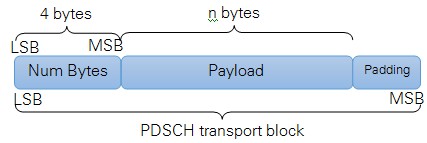
The MAC packet format is proprietary and shown in Figure 10. The PDSCH transport block size is defined according to [3] tables 7.1.7.1-1 and 7.1.7.2.1-1. It depends on the used modulation and coding scheme (MCS) and the number of resource blocks allocated for the PDSCH.
For each subframe the simple MAC implementation checks the fill state of the payload data FIFO which is filled with user-defined data from the host. Depending on the buffer fill state and the number of PDSCH transport block bits usable in the current subframe, the MAC determines the number of payload bytes which can be effectively transmitted by the PDSCH transport block. Based on this the content of the actual PDSCH transport block is composed. It starts with a 4 byte long MAC header which contains the number of effectively transmitted payload bytes. The second part is the payload itself. If necessary zero padding bits are added to fill up the PDSCH transport block to the configured size.
Figure 10: MAC Packet Structure
2.3.5. Uplink MAC Packet for Feedback Information
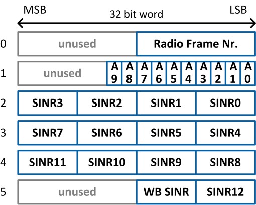
The content of the uplink transport blocks is composed based on the same MAC packet format as it is described for the downlink (see Figure 10 above). The actual “payload” portion is filled with downlink feedback information. As shown in Figure 13, each “payload” portion of an uplink MAC packet comprises 6 words of 32 bits, i.e. 192 bits in total. Unused bits are set to zero.
Figure 11: Feedback Information Packet Format
The feedback information is generated by the UE host implementation (UE feedback MAC) based on results provided by the UE downlink receiver. The following feedback information is provided:
- Radio Frame Number: A counter value from 0 to 1023 which is increased for each radio frame. It corresponds to the system frame number (SFN) defined in the LTE standard with the difference, that the timing is generated on the UE side and not dictated from the eNodeB using system information.
- A0 – A9: the DL ACK/NACK/DTX information for the latest 10 subframes providing information about the success of the PDSCH reception.
The values are encoded as a 2 bit number:- 0 = NACK (PDSCH was received with CRC error)
- 1 = ACK (PDSCH was received with CRC ok)
- 2 = DTX (no PDSCH was decoded because of missing or invalid DCI message)
- 3 = undefined
- Subband and wideband signal-to-interference noise ratio (SINR) in dB
- Subband size used for SINR calculation: 8 PRBs
- Subband numbering:
- SINR0 is subband SINR for PRBs 0..7, SINR1for PRBs 8..15, etc.
- SINR WB is the wide band SINR calculated over all subbands.
- Fixed point format: 8bits signed fixed-point number with 6 integer and 2 fractional bits (range -32.00 dB to +31.75 dB)
- SINR calculation is based on the CRS- or UERS-based channel estimates provided by the downlink receiver, for further details see section 2.3.5.1.
- When using UERS, the resource block allocation is currently not taken into account for SINR calculation. As UERS are only transmitted on allocated PRBs, SINR calculation results on not or only partially allocated subbands are undefined (i.e. in most cases less than the actual channel quality). Wideband SINR value is also undefined if not all subbands are fully occupied.
2.3.5.1. SINR estimation algorithm
The SINR estimation algorithm is based on filtering the potentially noisy channel estimates derived for the CRS subcarriers or the UERS subcarriers, respectively.
The noisy least squares (LS) channel estimates obtained for the reference symbol carriers are filtered by a de-noising lowpass filter to obtain LS channel estimates with reduced noise. The implemented prototype de-noising filter is a raised cosine filter with nine taps and the following filter coefficients.
| Coefficient Index | Coefficient Value |
|---|---|
| 0 | 0 |
| 1 | -0.061235467 |
| 2 | 0 |
| 3 | 0.306177333 |
| 4 | 0.510116268 |
| 5 | 0.306177333 |
| 6 | 0 |
| 7 | -0.061235467 |
| 8 | 0 |
The averaged signal power of the difference between the noisy channel estimates and their lowpass filter complements can be taken as raw estimate for the noise variance, i.e. it can be considered as scaled version of the actual noise variance in the given frequency band or sub-band.
Averaging the squared magnitudes of the low-pass filtered channel estimates delivers a raw estimate of the mean channel power gain.
Based on the known reference signal transmit power, the raw estimate of the mean channel power gain, and the raw estimate of the noise variance a raw CINR estimate can be derived.
Because both the raw mean channel power gain estimates and the raw noise variance estimates are biased, the raw SINR estimates are biased. Notice that especially the bias of the noise variance estimates bias strongly depends on the actual noise variance. That's why a mapping function has to be applied to map the biased raw SINR estimates to the final "unbiased" SINR estimates.
This mapping function has been derived by means of calibration simulations and measurements. It has been approximated by the following two linear functions (valid for a target SINR range between -6 dB to 30 dB):
SINR/dB = 1.8 * SINRraw/dB - 10.2 for -6 ≥ SINRraw/dB < 6
SINR/dB = 1.1 * SINRraw/dB - 6 for 6 ≤ SINRraw/dB ≤ 30
Note: To further improve the provided SINR estimates an additional look-up table based fine-calibration stage is implemented in the LTE application framework. The underlying look-up table has been derived by fine-calibration measurements.
Implementation Details
3.1. Architectural Overview
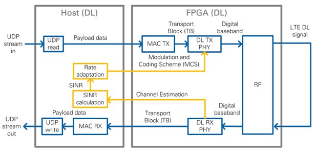
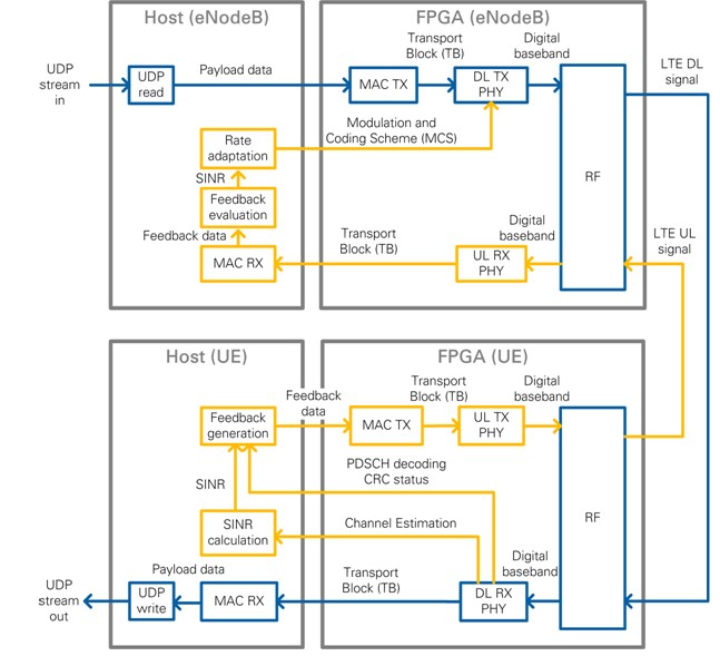
Figure 12 and Figure 13 show the block diagram of the system in the DL, eNodeB, and UE operation modes. Data streams that require high data rates for data transfer between host and FPGA are implemented as DMA FIFOs. These streams include the payload and uplink data from host to FPGA and the received PDSCH/PUSCH transport blocks from FPGA to host. IQ samples for constellation and spectrum display as well as the channel estimation values are also transferred from FPGA to host using DMA FIFOs. Further status information are transferred to the host by reading the indicator values.
Figure 12: Block Diagram of the System in DL Operation Mode (Single-Device Setup)
Figure 13: Block Diagram of the System in eNodeB/UE Operation Mode (Double-Device Setup)
The components shown in Figure 12 and Figure 13 perform the following tasks:
- UDP read—Reads data, provided by an external application, from an UDP socket. The data is used as payload data in the Transport Block (TB) which is then encoded and modulated as a LTE downlink (DL) signal by the downlink transmitter (DL TX PHY).
- UDP write—Writes the payload data, which was received and decoded from the LTE downlink (DL) signal by the downlink receiver (DL RX PHY), to an UDP socket. The data can then be read by an external application.
- MAC TX—A simple MAC implementation which adds a header to the Transport Block (TB) containing the number of payload bytes. The header is followed by the payload bytes and the remaining bits of the Transport Block are filled with padding bits.
- MAC RX—Disassembles the Transport Block (TB) and extracts the payload bytes.
- DL TX PHY—Physical layer (PHY) of the downlink (DL) transmitter (TX). Encodes the physical channels and creates the LTE downlink signal as digital baseband I/Q data. This includes: encoding of the control channel (PDCCH), encoding of the data channel (=shared channel, PDSCH), resource mapping, OFDM modulation.
- DL RX PHY—Physical layer (PHY) of the downlink (DL) receiver (RX). Demodulates the LTE downlink signal and decodes the physical channels. This includes: primary synchronization sequence (PSS) based synchronization, OFDM demodulation, resource demapping, channel estimation & equalization, decoding of the control channel (PDCCH), decoding of the data channel (=shared channel, PDSCH).
- UL TX PHY—Physical layer (PHY) of the uplink (UL) transmitter (TX). Encodes the physical channels and creates the LTE uplink signal as digital baseband I/Q data. This includes: encoding of the data channel (=shared channel, PUSCH), resource mapping, OFDM modulation.
- UL RX PHY—Physical layer (PHY) of the uplink (UL) receiver (RX). Demodulates the LTE downlink signal and decodes the physical channels. This includes: OFDM demodulation, resource demapping, channel estimation & equalization, decoding of the data channel (=shared channel, PUSCH).
- SINR calculation—Calculation of the Signal-to-Interference-Noise-Ratio (SINR) based on the channel estimation which was used for PDSCH decoding: channel estimation is either based on cell-specific reference signals (CRS) or on UE-specific reference signals (UERS)
- Rate adaptation—Sets the Modulation and Coding Scheme (MCS) depending on the measured/reported Signal-to-Interference-Noise-Ratio (SINR). The aim is to ensure to keep the block error rate (BLER) of the PDSCH decoding low.
- Feedback generation—Creates a feedback message with contains the measured subband and wideband SINR as well as the ACK/NACK information (=CRC result of the PDSCH decoding) of the previously received radio frame.
- Feedback evaluation—Extracts the subband and wideband SINR as well as the ACK/NACK information from the feedback message.
3.2. FPGA Implementation Overview
This LTE Application Framework is based on the target specific sample streaming project (“PXIe USRP RIO 40 MHz BW Single-Device Streaming” for USRP RIO 40 MHz BW or “PXIe USRP RIO 120 MHz BW Single-Device Streaming” for USRP RIO 120 MHz BW or “PXIe NI-579xR Streaming” for FlexRIO/FAM). The sample streaming project contains the basic logic to interface with the A/D converter (ADC) and D/A converter (DAC) registers. It also performs digital up and down conversion, configuration for the front-ends, and RF impairment correction.
In the LTE Application Framework, the processing blocks for the downlink and uplink transmitter and receiver are implemented on the FPGA directly. They exchange the baseband data with the RF interface using target-scoped FIFOs. The processing on the FPGA has advantages as it provides lower latency and therefore enables real-time physical layer processing. This approach is different from the sample streaming project where the digital baseband data is sent to or received from the host which is then responsible for all channel encoding and decoding.
Figure 14 shows the structure of the FPGA implementation for the different operation modes. The outer boxes (highlighted in light gray) represent single-cycle timed loops which implement clock-driven logic. The inner boxes correspond to the high-level blocks described in the architectural overview. The transmitter loop receives payload data from the host via a DMA FIFO, performs channel encoding and generates the TX baseband signal which is passed to the RF loop for up conversion. The RF loop is inherited from the sample streaming project. It also performs down conversion of the RX baseband signal that is passed to the receiver loop for channel decoding. The decoded transport blocks are sent to the host using a DMA FIFO.
Figure 14: Implemented FPGA Loops for Different Operation Modes
3.2.1. RF Interface
3.2.1.1. Digital Upconversion and RF Impairment Correction
The transmit part of the RF loop is shown in Figure 15. The first block is the Fractional Interpolator which converts the standard LTE rate of 30.72 MS/s to the DAC sample rate (120 MHz for USRP RIO 40 MHz BW, 200 MHz for USRP RIO 120 MHz BW, 130 MHz for FlexRIO/FAM). Next, the frequency shift module performs a fine frequency shift which is automatically configured by the RF driver. The I/Q imbalance correction uses coefficients determined during manufacturing and stored in the device EEPROM.
Figure 15: Digital Upconversion Block Diagram
3.2.1.2 Digital Downconversion and RF Impairment Correction
The receive part of the RF loop is shown in Figure 16. It corrects I/Q impairments in the baseband signal, performs fine-frequency adjustments and performs sample rate conversion. I/Q imbalance correction uses coefficients determined during manufacturing and stored in the device EEPROM. A decimator converts the sample rate from the ADC sample rate (120 MHz for USRP RIO 40 MHz BW, 200 MHz for USRP RIO 120 MHz BW, 130 MHz for FlexRIO/FAM) to the standard LTE rate of 30.72 MS/s. The LTE Application Framework also includes a DC suppression to compensate for the DC offset. This module averages over time to remove the DC portion of the signal.
Figure 16: Digital Downconversion Block Diagram
3.2.2. Downlink Transmitter
3.2.2.1. Overview
The Downlink Transmitter is implemented by the FPGA top-level variants eNodeB and Downlink only (DL). In the block diagrams of Figure 12 and Figure 13, it corresponds to the “DL TX PHY” block.
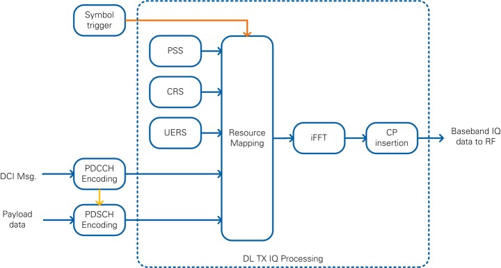
As shown in the simplified block diagram in Figure 17, it performs the following tasks:
- Physical Downlink Control Channel (PDCCH) encoding
- Physical Downlink Shared Channel (PDSCH) encoding
- Mapping to resource elements
- iFFT conversion + CP conversion (OFDM modulation)
The following reference signals and physical channels are mapped:
- Primary Synchronization Signal (PSS)
- Cell-Specific Reference Signal (CRS)
- UE-specific Reference Signal (UERS), if enabled
- Physical Downlink Control Channel (PDCCH)
- Physical Downlink Shared Channel (PDSCH)
Figure 17: Simplified Block Diagram of Downlink Transmitter
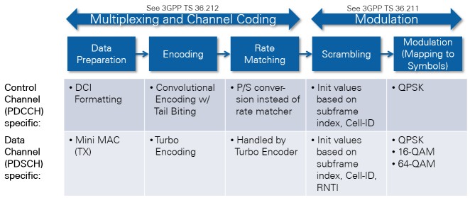
Channel Encoding is performed for the PDCCH and PDSCH physical channels as shown in Figure 18. The encoding is performed for each downlink subframe by the FPGA implementation which allows real-time operation. The other signals are read out from look-up tables (LUTs).
Figure 18: Channel Encoding Performed in the Downlink Transmitter
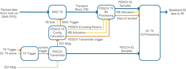
An extended block diagram which represents the actual implementation is shown in Figure 19. It shows the data path (blue color), the configuration signals (yellow signal) and the triggering signals (orange color).
Figure 19: Block Diagram of Downlink Transmitter showing Data, Trigger and Control Paths
If the Downlink Transmitter is active and if it receives a TX trigger signal, it generates symbol triggers for one complete radio frame (10 subframes à 14 symbols = 140 symbols). The TX trigger signal is provided from a register which is written in the DAC/ADC loop. This ensures synchronization between both loops and compensates eventual clock drifts. The symbol trigger is passed through the rest of the chain and causes the modules to produce data: a subframe trigger is derived for the PDCCH and PDSCH Transmitters which produce enough data for one subframe. The DL TX IQ uses the symbol trigger and generates time-domain IQ samples for one OFDM symbol.
The PDCCH Transmitter performs channel encoding for the physical downlink control channel (PDCCH). The DCI message serves as input data. As shown in Figure 3 it contains the modulation and coding scheme (MCS) and the resource block allocation (RB Allocation). The resulting PDCCH IQ samples are written to a FIFO inside the “TX IQ Processing” module.
The DCI message is also input to the module which calculates the PDSCH transmitter configuration parameters (PDSCH TX Config Calculation). It performs two tasks: first, it calculates the transport block (TB) size and triggers the MAC TX. Second, it calculates the PDSCH Encoding parameters, extracts the resource block (RB) allocation and triggers the PDSCH TX Bit Processing module.
The MAC TX assembles the transport block in the format as shown in Figure 10. The payload data is read from the host via a host-to-target DMA FIFO.
The PDSCH TX Bit processing module includes the channel encoding, scrambling and modulation of the physical downlink shared channel (PDSCH). It uses the modulation and coding scheme (MCS) which is defined inside the DCI message. The resulting PDSCH IQ samples are written to a FIFO inside the “TX IQ Processing” module.
The TX I/Q processing module is triggered after the PDCCH and PDSCH I/Q samples for the current subframe were generated. It includes the resource mapping that assembles all 1,200 subcarriers of the current symbol. The index generator generates the timing information for each sample of the current OFDM symbol, such as subcarrier, resource block, OFDM symbol and subframe index. Depending on the current timing information, the index-to-channel mapping decides for each subcarrier, which reference signal or physical channel is mapped to it. The PSS sync sequence, the cell-specific reference symbols (CRS) and the UE-specific reference symbols (UERS) are precalculated and stored in a look-up table (LUT). The PDCCH and PDSCH IQ samples are read from a FIFO that was filled with all I/Q samples for the current subframe before the TX I/Q processing module was triggered. After combining all channels, the DC gap is inserted and whitespace is added so that the resulting number of samples equals the FFT size of 2,048. The inverse fast Fourier transformation (iFFT) converts the frequency domain data into the time domain. Finally, the cyclic prefix is attached to the output of the iFFT. The resulting time-domain signal is transferred to the RF loop using a FIFO.
PDCCH Transmitter
The PDCCH Transmitter creates all QAM symbols for the PDCCH channel. The contained blocks are illustrated in Figure 20.
Upon reception of the symbol trigger, the DCI message is generated based on the configuration from the host. The message is encoded and a CRC is attached. The DCI multiplexer module shifts the generated symbols to the correct position within the PDCCH channel. Afterwards the whole channel data is scrambled and interleaved. After applying the QPSK-Modulation to the symbols, the PDCCH I/Q-samples are fed into a FIFO that stores them until they are picked up by the resource grid generation.
Figure 20: PDCCH Transmitter Block Diagram
PDSCH Transmitter
The PDSCH transmitter converts the user data from the host to QAM symbols for the PDSCH channel. The blocks of this processing chain are shown in Figure 21. A basic MAC implementation adds a proprietary MAC header to the beginning of each PDSCH transport block. The remaining transport block is filled with as much user data as available from the host FIFO. If necessary, zero padding bits are added to fill the remaining portion of the transport block. The PDSCH Encoder uses the LTE DL Channel Encoder from Xilinx. The output of the core is scrambled according to the LTE specification. Afterwards the QAM modulation is applied. The MCS value on the host sets the modulation scheme. After the modulation, the PDSCH QAM symbols are fed into a FIFO that holds these values until they are pulled into the resource grid.
Figure 21: PDSCH Transmitter Block Diagram
3.2.3. Downlink Receiver
3.2.3.1. Overview
The Downlink Receiver is implemented by the FPGA top-level variants UE and Downlink only (DL). As shown in the simplified block diagram in Figure 22, it performs the following tasks:
- Synchronization and carrier frequency-offset (CFO) compensation
- CP removal + FFT conversion (OFDM demodulation)
- Demapping of the resource elements to the different physical channels
- CRS-based channel estimation and equalization
- UERS-based channel estimation and equalization
- Physical Downlink Control Channel (PDCCH) decoding
- Physical Downlink Shared Channel (PDSCH) decoding
The following reference signals and physical channels are demapped:
- Primary Synchronization Signal (PSS)
- Cell-Specific Reference Signal (CRS)
- UE-specific Reference Signal (UERS)
- Physical Downlink Control Channel (PDCCH)
- Physical Downlink Shared Channel (PDSCH)
Figure 22: Simplified Block Diagram of Downlink Receiver
The downlink receiver (DL RX) receives the IQ samples in time domain from the RF loop which is derived from the sample streaming project. It performs the IQ impairments correction, digital down conversion, frequency shift and the down conversion from the ADC sample rate to the LTE sampling frequency of 30.72 MHz. The first processing step in the downlink receiver loop is the synchronization. The primary synchronization signal (PSS) is used for radio-frame synchronization and carrier frequency-offset (CFO) compensation.
The cell-specific reference signals (CRS) are used for channel estimation and equalization. Per default, the CRS equalized samples are used for PDCCH and PDSCH decoding. The UE-specific reference signals (UERS) can be used optionally. The UERS based channel estimation and equalization runs in parallel to the CRS based channel estimation and equalization. If UERS are enabled, the UERS equalized samples are used for PDSCH decoding.
The PDCCH decoder decodes the physical downlink control channel (PDCCH). It includes the downlink control information (DCI message).
The PDSCH decoder decodes the physical downlink shared channel (PDSCH). The PDSCH configuration parameters are derived from the received DCI message. It determines the resource block allocation, i.e. which subcarriers are filled with PDSCH, and the modulation and coding scheme (MCS). The decoded PDSCH transport blocks are written to the host using a target-to-host DMA FIFO.
The following sections describe each of the blocks from Figure 22 in more detail.
3.2.3.2. Radio Frame Synchronization
Data is transferred from the RF loop to the downlink receiver (DL RX) loop using a FIFO. This block’s main purpose is to determine the start of the LTE radio frame and to align the received time-domain signal accordingly. Another task of this block is the compensation of carrier-frequency offset. Only if both the sync signal was detected and the CFO was compensated, full radio frames are passed to the subsequent processing blocks.
The components of the Radio Frame Synchronization block are shown in Figure 23. Synchronization and CFO compensation are achieved by continuous measurement of both an autocorrelation and a cross correlation. LTE signals contain a primary synchronization signal (PSS), which is detected by two FIR filters (real and imaginary part) that calculate the cross correlation. This operation is executed on a reduced sample rate of 1.92 MS/s which is the result of a decimation by 16. For each radio frame, the cross correlation peak is detected. To avoid misdetection, a validation unit checks that the peak amplitude is 8 times higher than the average energy of the cross correlation. Additionally, three consecutive peaks are required and the peak position may not drift more than 5 samples.
In parallel to the cross correlation, an autocorrelation is performed on the full sample rate. Its purpose is to locate the OFDM symbol boundaries. The autocorrelation value is calculated by multiplying the IQ samples values with delayed and conjugated IQ samples and accumulation. A division by the energy normalizes the value. A peak is detected on the highest amplitude if more than 32 samples exceed a specified threshold and the distance to the last peak is more than 2,160 samples.
Another function of the radio frame synchronization block is the measurement and compensation of the carrier frequency offset (CFO). The integer frequency offset (IFO) estimation is calculated based on the distance between the cross-correlation and the autocorrelation peak. Only if it is below a certain threshold, the IFO is assumed to be zero. The fractional frequency offset (FFO) is calculated based on the phase of the autocorrelation peak. The resulting CFO estimate is obtained by adding the IFO and FFO estimates. To prevent noisy estimates from sifting the estimate too much, the fractional part is multiplied with a “CFO factor” before it is used for updating the CFO estimate. When the synchronization is found, the new CFO estimate is only applied at the start of a radio frame. For debug purposes, a “static CFO” value can be configured which overrides the CFO estimation.
After multiple PSS signals are detected consecutively and the IFO estimation is complete, the Timing Adjustment block calculates the position of the start of the radio frame. The Radio Frame Alignment block uses this position to pass an entire time-aligned radio frame to the subsequent modules. The “FFT window timing advance” parameter can be used to set the amount of samples that the receiver should cut into the cyclic prefix. This parameter together with the parameters mentioned before are part of the “sync configuration” cluster and can be set from the host.
If PSS or OFDM peaks are missing, the IFO Estimation block invalidates at least one radio frame of samples. In this case the samples are not passed to the subsequent modules.
Figure 23: Radio Frame Synchronization Block Diagram
3.2.3.3. DL RX IQ Processing
This module reads the radio-frame aligned signal in time domain and outputs the channel-equalized subcarriers that are associated to the physical channels.
As shown in Figure 24, it includes the following functional blocks:
- Cyclic prefix (CP) removal
- FFT conversion
- Resource demapping
- Cell-specific reference signal (CRS) based channel estimation and equalization
- UE-specific reference signal (UERS) based channel estimation and equalization
Figure 24: Block Diagram of DL RX IQ Processing
An internal FIFO is used to decouple the incoming samples from the rest of the processing chain. The throttle control module waits until enough samples for one complete OFDM symbol (FFT size + CP) are available before it passes them as a consecutive stream to the next modules.
The next module is the cyclic prefix (CP) removal which removes the valid flag from the samples belonging to the cyclic prefix. The 2,048 remaining samples are sent to a Xilinx FFT. The output of the FFT are 2,048 the subcarriers in frequency domain. The resource mapper first selects the 1,200 allocated subcarriers by removing the surrounding whitespace and the DC carrier in the center. Afterwards, it generates the timing information for each sample and the resource grid by marking each sample for its corresponding channel by using a Boolean cluster. The resource mapping is based on a fixed frame structure configuration described in the LTE specifications. All subsequent modules use this Boolean cluster with elements for each LTE channel to determine if this sample is relevant.
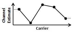
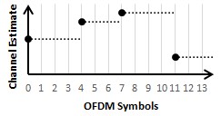
The FFT output data is fed into two separate channel estimation blocks running in parallel. The first channel estimation is based on the CRS. The channel estimate values are calculated by conjugate complex multiplications. A linear interpolation is applied in frequency domain between adjacent reference symbols, as shown in Figure 25. On the edges of the symbol, the nearest estimated value is replicated (zero order hold). OFDM symbols not containing CRS sequences rely on the last channel estimation (zero order hold in time; as shown in Figure 26).
Figure 25: Channel Estimation over Frequency Error loading
Figure 26: Channel Estimation over Time
The second channel estimation is based on the UERS. These pilots are transferred in each physical resource block (PRB) assigned to the PDSCH addressed to the UE. At this point, there is no knowledge about the PRB allocation. Therefore the channel estimation is done on each PRB. The same resource elements can use multiple UERS, so the averaging over one subframe is used in the time domain to cancel other possible sequences (multi-user interference cancellation). In the frequency domain, linear interpolation is used within the PRBs with zero-order hold applied at the edges.
The channel estimation is delivered sample by sample to the channel equalization modules parallel to the data. The channel equalization determines the result from the data sample d and the channel estimate e by using the following equation:
3.2.3.4. PDCCH Receiver
The PDCCH Receiver works on the output of the CRS-based channel equalization for the first OFDM symbol of each subframe (CFI fixed to 1). It decodes the downlink control information (DCI) for the UE given in the PDCCH channel. The block diagram is shown in Figure 27.
The PDCCH receiver first extracts the PDCCH subcarriers from CRS equalized subcarriers. This is done by evaluating the channel map which is passed to the module in addition to the subcarrier IQ data. An LLR demapper translates the symbols into soft bits, which are deinterleaved and descrambled by the given system and timing parameters.
After this step, the DCI demultiplexer extracts one DCI message from the PDCCH. The CCE offset parameter can be used to determine the DCI message location. The DCI decoder uses the Xilinx Viterbi Decoder Core to decode the DCI transport block bits from the given soft bits. The checksum of the cyclic redundancy check (CRC) is calculated on the transport block. If this value matches the configured radio network temporary identifier (RNTI), the message is marked as valid.
The valid DCI message is interpreted according to the implemented DCI format (see Figure 3). A validation module invalidates the DCI message in case the content is not supported, e.g. when MCS > 28. It is also invalidated if a downlink assignment is received outside a downlink subframe.
Figure 27: PDCCH Receiver Block Diagram
3.2.3.5. PDSCH Receiver
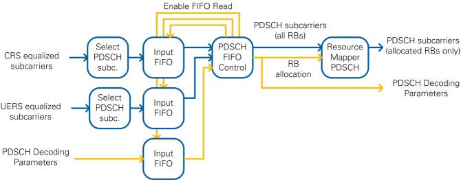
Depending on the system configuration, either CRS or UERS equalized QAM symbols are used. The selection is performed inside the PDSCH Sample Select module which is shown in Figure 28. This module buffers the incoming subcarrier data in FIFOs until a valid PDSCH Decoding Parameter configuration is received from the PDCCH Decoding. In case of CRS-equalized subcarriers, the first subframe is received before the PDSCH Decoder configuration. In case of UERS-equalized it is received later because of the higher latency of the UERS channel estimation. The PDSCH subcarriers provided by the PDSCH FIFO Control module comprise the PDSCH subcarriers of all 100 resource blocks. Another resource demapper marks the PDSCH QAM symbols as valid or invalid based on the RB allocation from the decoded DCI message which is provided as part of the PDSCH Decoding parameters.
Figure 28: PDSCH Sample Select Block Diagram
The selected PDSCH subcarriers and the corresponding PDSCH Decoding Parameter are passed to the PDSCH Bit Processing module which is shown in Figure 29.
The valid symbols are interpreted as softbits in the LLR demapper. These softbits are descrambled using the cell parameters and the RNTI. A Scrambler initialization module calculates the initialization value of the shift register which corresponds to 1600 iterations in just 32 clock cycles.
The PDSCH Transport Blocks are decoded inside the PDSCH Channel Decoder. It includes the Xilinx LTE UL Channel Decoder core which is configured to perform Turbo Decoding. The necessary parameters (TB size, code block size, number of code blocks) are calculated on the FPGA based on the received DCI message and the configured system settings. The hard bits from the decoder are transferred to the host using a dedicated FIFO. Another FIFO writes the decoding status information to the host.
Figure 29: PDSCH RX Bit Processing Block Diagram
3.2.4. Uplink Transmitter
The Uplink Transmitter is implemented by the FPGA top-level UE. In the block diagrams of Figure 13, it corresponds to the “UL TX PHY” block.
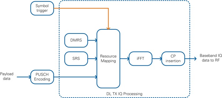
As shown in the simplified block diagram in Figure 30, it performs the following tasks:
- Physical Uplink Shared Channel (PUSCH) encoding
- Mapping to resource elements
- iFFT conversion + CP conversion (OFDM modulation)
The following reference signals and physical channels are mapped:
- Demodulation Reference Signal (DMRS)
- Sounding Reference Signal (SRS), if enabled
- Physical Uplink Shared Channel (PUSCH)
Figure 30: Simplified Block Diagram of Uplink Transmitter
Channel Encoding is performed for the PUSCH as shown in Figure 31. The encoding is performed for each uplink subframe by the FPGA implementation which allows real-time operation. The other signals are read out from look-up tables (LUTs).
Figure 31: Channel Encoding Performed in the Uplink Transmitter
3.2.5. Uplink Receiver
The Uplink Receiver is implemented by the FPGA top-level variant eNodeB. As shown in the simplified block diagram in Figure 32, it performs the following tasks:
- CP removal + FFT conversion (OFDM demodulation)
- Demapping of the resource elements to the different physical channels
- DMRS-based channel estimation and equalization
- Physical Uplink Shared Channel (PUSCH) decoding
The following reference signals and physical channels are demapped:
- Demodulation Reference Signal (DMRS)
- Sounding Reference Signal (SRS), if enabled
- Physical Uplink Shared Channel (PUSCH)
Figure 32: Simplified Block Diagram of Downlink Receiver
The uplink receiver (UL RX) receives the IQ samples in time domain from the RF loop which is derived from the sample streaming project. It performs the IQ impairments correction, digital down conversion, frequency shift and the down conversion from the ADC sample rate to the LTE sampling frequency of 30.72 MHz.
In contrast to the downlink receiver (DL RX), synchronization is not performed because the UE is required to send the uplink subframe with the correct timing. Therefore the incoming I/Q samples are already time-aligned.
The demodulation reference signals (DMRS) are used for channel estimation and equalization. The PUSCH decoder decodes the physical downlink shared channel (PUSCH). The PUSCH configuration parameters are calculated based on the MCS and RB allocation parameters which are set from the host. The decoded PUSCH transport blocks are written to the host using a target-to-host DMA FIFO. The submodules used for the uplink receiver are very similar to the submodules used for the downlink receiver. Refer to this section for more infomration about the implementation of these submodules.
3.2.6 Clocking Considerations
There are three main clock domains used inside the FPGA: 40 MHz onboard clock, 120 MHz, 130 MHz, or 200 MHz Sample Clock, and 192 MHz baseband clock.
The configuration loops are connected to the 40 MHz clock domain. The configuration information is set prior to execution and used as constants elsewhere in the design.
All LTE baseband processing loops run at a clock rate of 192 MHz. The ADC and DAC interfaces run at the Sample Clock rate, in addition to the sample rate converters that create the 30.72 MS/s I/Q data. The 192 MHz processing clock and Sample Clock are not synchronized, and this difference is accounted for in the design. The processing performed in the 192 MHz domain has enough margin to account for frequency tolerances between the 192 MHz clock and the Sample Clock.
The downlink transmitter chain uses a synchronization mechanism to keep the baseband processing aligned and to avoid any under- or overflows of the FIFO that transfers data between the two clock domains. The sample clock domain is used as the absolute time reference. A trigger is generated in the sample clock domain every 10 milliseconds (for each radio frame). This trigger is sent to the 192 MHz processing domain to initiate the creation of a new radio frame. The FIFO between the two clock domains guarantees a constant data rate for the digital up conversion module.
For testing purposes, there is an internal loopback FIFO on the DL FPGA that you can use to bypass the RF by directly transferring samples from the DL TX to the DL RX baseband processing. The internal loopback is disabled by default and can be enabled from the host.
3.3 Host Implementation Overview
The LTE Application Framework provides three sample host implementations which cover all important features of the LTE Application Framework. As described in the section 2.1, three different host implementations are provided:
- Downlink (DL)—Can be used to establish a downlink link in either a single-device setup or a double-device setup.
- eNodeB:
- Provides the base station (eNodeB) side in a double-device setup.
- Implements the downlink transmitter (DL TX) and the uplink receiver (UL RX) of an eNodeB.
- UE:
- Provides the user equipment (UE) side in a double-device setup.
- Implements the downlink receiver (DL RX) and the uplink transmitter (UL TX) of a UE
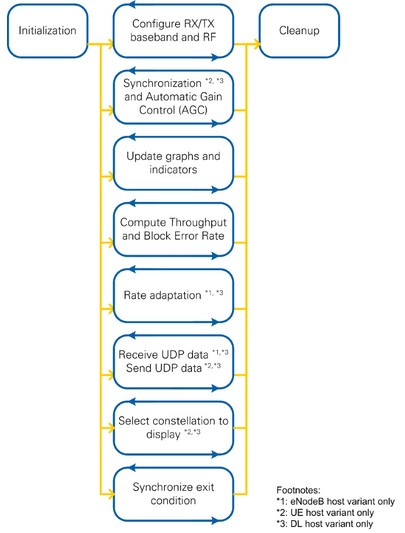
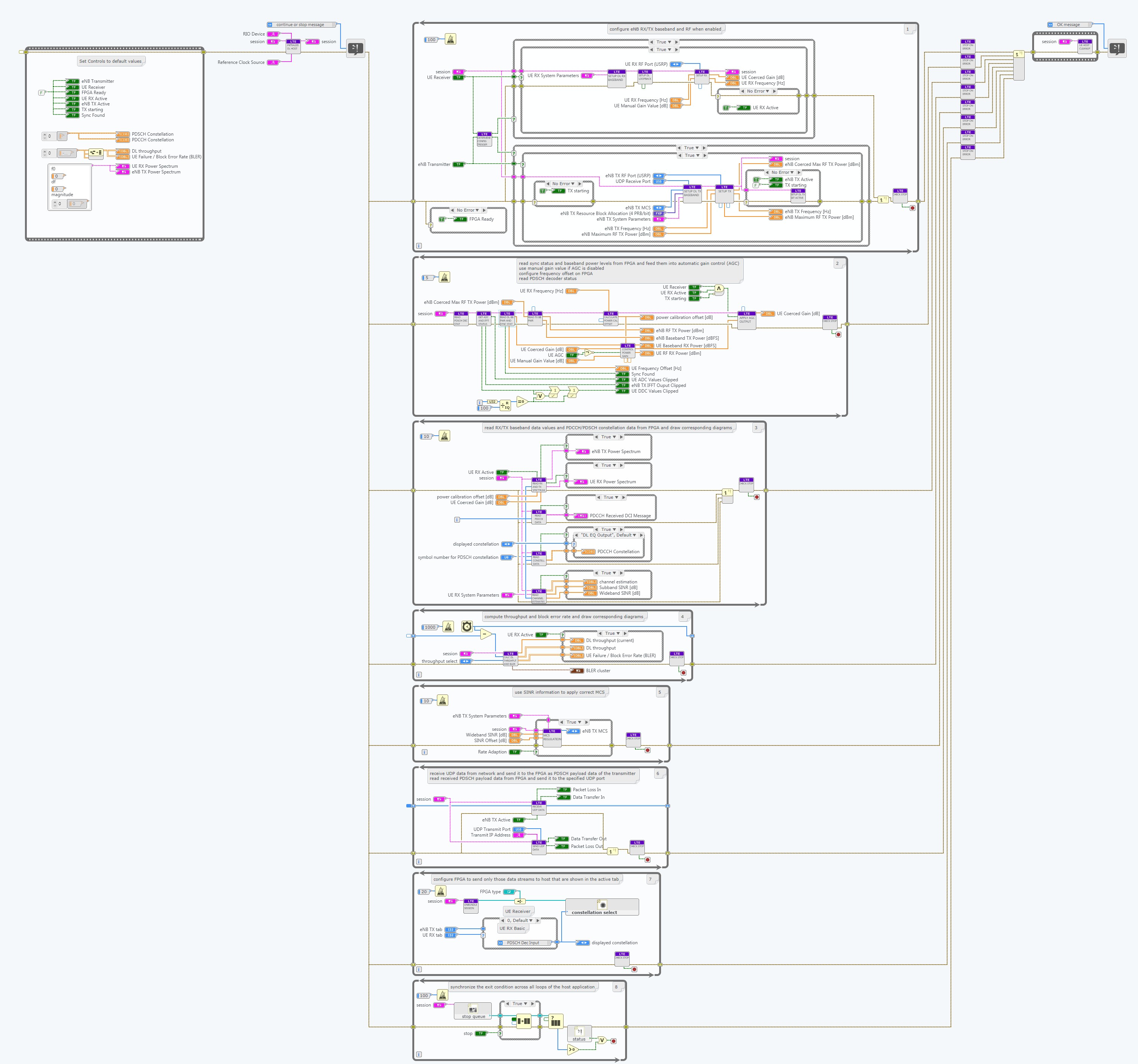
Each host implementation interfaces with the bitfile that was built from the corresponding FPGA implementation. It demonstrates the main functionalities for each implementation. This functionality includes configuration of the FPGA target, exchanging payload data, and monitoring the system status. As shown in the schematic overview of Figure 33, each host implementation is split into an “Initialization” part, several processing loops and a “Cleanup” part. Figure 34 shows a screenshot of the LabVIEW G code.
All parts and processing loops are further described in the next sections.
Figure 33: Host Block Diagram – Schematic Overview
Figure 34: Host Block Diagram – Screenshot of LabVIEW G code
3.3.1 Initialization, Synchronize Exit Condition and Cleanup
The entry point of the code is the initialization block. It sets several controls and indicators to default values. Also, it prepares the session cluster by starting the necessary queues and loading the FPGA bitfile to the configured RIO device. All processing loops use this session cluster during execution to exchange data or to access the FPGA resources.
All processing loops are implemented as while loops which run in parallel during the execution of the host VI. A dedicated “stop” queue is used to synchronize the stop condition across all loops. The “synchronize exit condition” loop checks it the “Stop” button is pressed and accordingly sets the stop condition. The stop condition is also set in case an error occurred in any of the processing loops. After all processing loops were stopped, the handles from the session are closed, i.e. the queues are stopped and the FPGA reference is closed.
3.3.2 Configure RX/TX Baseband and RF
This loop handles the configuration of the target specific RF and the LTE processing chains. After changes to the RX or TX enable switches, the required parameters are passed to the LTE FPGA processing chain using the settings presented on the front panel, e.g. the Modulation and Coding Scheme (MCS) and the Resource Block Allocation are configured when the downlink transmitter (DL TX) is enabled. After the LTE processing parameters were written to the FPGA, the RF chain is configured and started. Some error cases are caught and presented to the user in dialog boxes.
3.3.3 Synchronization and Automatic Gain Control (AGC)
The loop continuously monitors the received signal power and adjusts the gain for the RX path accordingly. It reports the status of the radio frame synchronization on the FPGA and updates the overflow indicators on the front panel.
This loop also reads the PDSCH decoding status (DL, UE host variants) or the PUSCH decoding status (eNodeB host variant). This information is needed for the outgoing UDP Stream and the throughput calculation. Therefore the elements which are read from the PDSCH/PUSCH decoding status FIFO are duplicated and written to multiple queues.
3.3.4 Update Graphs and Indicators
This loop reads and processes status information from the FPGA and updates the associated graphs and indicators on the host front panel. E.g. it reads the baseband signal of the associated RX or TX processing chain, calculates the power spectra and updates the corresponding graphs. This loop also updates the constellation diagram which is shown on the currently selected tab. For the DL and UE host variant, it also reads the current channel estimation, calculates both the subband and wideband SINR from it and updates the associated graphs and indicators.
3.3.5 Compute Throughput and Block Error Rate
This loop calculates the throughput and the Block Error Rate based on the state of several queues which are filled by the other processing loops.
The queues are emptied on a fixed time basis (1000 ms) and the elements are accumulated as follows:
ThroughputUser Data = ∑1000 msnPayload Bits
ThroughputPDSCH (CRC OK) = ∑1000 ms|CRC OKTB Size
ThroughputPDSCH (Overall) = ∑1000 msTB Size
Where nPayload Bits is the number of the payload bits per received transport block. This value is the result of the MiniMAC header interpretation. TB Size is the size of the received transport block. The ThroughputPDSCH (CRC OK value considers only the transport blocks which were received successfully, without CRC errors. The PDSCH (overall) throughput accumulates the sizes of all transport blocks independently of the CRC status.
The sync failure rate, PSync Failure, and the PDCCH and PDSCH Block Error Rates (BLER) BLERPDCCH and BLERPDCCH are calculated as follows:
PSync Failure = 1 - PSync Successful, PSync Successful = nSync Successful/nSync Checked
BLERPDCCH = 1 - PSync Successful * PPDCCH Successful , PPDSCH Successful = nPDSCH, (CRC OK)/nPDSCH
BLERPDSCH = 1 - PSync Successful * PPDCCH Successful * PPDSCH Successful , PSync Successful = nPDCCH (CRC OK)/nPDCCH
Where nSync Successful is the number of times the sync was successful, and nSync Checked is the number the sync status was checked (inside the “Synchronization and AGC” loop).
nPDCCH is the number of decoded DCI messages, and nPDCCH (CRC OK) is the number of messages that were decoded successfully, without CRC errors.
nPDSCH is the number of decoded PDSCH transport blocks and nPDSCH (CRC OK) is the number of PDSCH transport blocks that were decoded successfully (i.e. without CRC errors).
3.3.6 Rate adaptation
The DL and the eNodeB host variants contain a rate adaptation that sets the Modulation and Coding Scheme (MCS) depending on the reported wideband SINR value. This value is either read directly from the FPGA (DL host variant) or received from the UE as part of the uplink feedback (eNodeB host variant). The implemented SINR-MCS mapping table is calibrated so that the resulting PDSCH BLER is around 10% if no offset is applied. The control “SINR Offset [dB]” can be used to apply an SINR offset which allows to achieve a lower PDSCH BLER value.
3.3.7 Receive UDP Data/Send UDP Data
In the eNodeB and DL host variant, this loop handles incoming UDP data, which is used as the payload data for downlink transmission (DL TX). The data is provided by an external application and read from the port number which is specified on the front panel. The data is pushed to the FPGA using a host to target FIFO.
In the UE and DL host variant, this loop also handles outgoing UDP data. This data stream represents the payload data which was received and successfully decoded from the downlink receiver (DL RX). After the data was transferred to the host using a target to host FIFO, the data is packed into a UDP stream and sent to an external application. The IP address and port number can be specified on the front panel.
3.3.8 Select Constellation to Display
For the UE and DL host variant, this loop checks which I/Q constellation is shown depending on the currently displayed tab. The associated physical channel is determined and requested from the FPGA. This step is necessary because a shared target-to-host DMA FIFO is used to transfer the IQ samples to the host.
Conclusion
The LabVIEW Communications LTE Application Framework provides a real-time LTE downlink and uplink including basic feedback mechanisms running on NI SDR hardware. This framework enables you to focus on a specific area of research by utilizing the existing link and only making changes or additions where desired.
Because of the flexibility of LabVIEW and the modularity of the framework, you can easily exchange portions of the design for prototyping new algorithms for future wireless systems. In addition, LabVIEW’s native interface between the host and the FPGA means that the design can be partitioned to profit from the parallel execution on the FPGA as well as calculations on the host.
The FPGA bitfiles shipped with the design are fully functional and support test modes with and without the RF. In addition, you can use external RF equipment, such as the NI vector signal transceiver (VST), to simulate interference and various channel conditions.
This application framework offers a variety of starting points for wireless research and prototyping.
Questions? Email us at labview.communications@ni.com.
Bibliography
[1] 3GPP, "TS36.211: Evolved Universal Terrestrial Radio Access (E-UTRA); Physical Channels and Modulation (Release 10), V10.7.0," 2013-02.
[2] 3GPP, "TS36.212: Evolved Universal Terrestrial Radio Access (E-UTRA); Multiplexing and channel coding (Release 10), V10.8.0," 2013-06.
[3] 3GPP, "TS36.213: Evolved Universal Terrestrial Radio Access (E-UTRA); Physical layer procedures (Release 10), V10.12.0," 2014-03.
