HSDIO Generation and Acquisition Synchronization
Overview
Contents
- HSDIO Generation and Acquisition Synchronization Overview
- HSDIO Architecture Overview
- Synchronizing Generation/Acquisition Tasks to Eliminate Round Trip Delay (RTD)
- Troubleshooting/FAQ
HSDIO Generation and Acquisition Synchronization Overview
Synchronizing HSDIO generation and acquisition tasks can present a challenge in many real-world applications. When using higher speed clocks and attempting to generate and acquire data synchronously, it is often not sufficient to simply start each task simultaneously with the same clock rate. Synchronizing HSDIO involves understanding several concepts about the architecture of the board, and the theory of why and how to use the features provided by software and hardware.
HSDIO Architecture Overview
Before understanding how to synchronize the timing engines on your HSDIO board, let’s begin by overviewing the architecture of the board and build on that knowledge as we move towards more technical synchronization details.
A. Pattern Generation and Acquisition Timing Engines
Each HSDIO board has a separate timing engine for acquisition and generation tasks. What this means is that the generation and acquisition tasks can make independent use of either the On Board Clock, External Clock, or Reference Clock. For example, the generation timing engine can run off the on board clock frequency generated by its internal oscillator, and the acquisition timing engine can run at a different frequency based on an external clock. They do not have to have any timing relationships between the two, although it is common and encouraged to phase align these signals.
The generation and acquisition engine can run off of the same on board clock frequency as well. To vary frequencies, you must have two different clock sources for each independent timing engine. It is not possible to vary the frequencies with only the single clocking resource on the board.
B. HSDIO Architecture Block Diagram
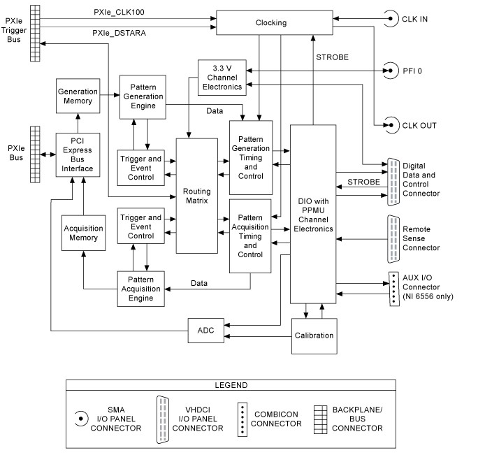
The following is a block diagram of the 6556 which shows a high level overview of the hardware architecture that is common to most HSDIO boards (This diagram will vary based on product family). From here, you can see the two timing engines and their pattern/event/trigger components. Also note the Clocking block, which sources a clock to each timing engine:
Figure 1: NI PXIe-6556/6555 Block Diagram
The important resources to note for synchronization are where your clocking sources are coming from, how you are triggering your device to begin sampling, how you are signaling your device is beginning generation (events), and the relationship between generation and acquisition.
C. Clocking Sources
There are three main clocking source options available to use: Sample Clock, Reference Clock, Static Timing
The Sample Clock is used to control the rate at which samples are generated or acquired. This clock can be sourced from the On Board Clock, CLK IN on the front panel of most HSDIO devices, or Strobe on the DDC connector.
To lock the On Board Clock to an external reference frequency, a Reference Clock source may be specified. The oscillator of an HSDIO board uses a PLL circuit to lock the On Board Clock to this known reference. This is most commonly used with one of the PXI backplane clocks, PXI_CLK10 or PXIe_CLK100, to phase lock all devices in a chassis to a single source. The reference clock can also be provided on a CLK IN front panel connector.
Static timing means using the generation and acquisition engines without a clock. This cannot be synchronized, as it is determined by the operating system which is inherently nondeterministic.
D. Events
A vital piece of the synchronization puzzle is when to begin a generation or acquisition task on each of the synchronized devices. This is achieved through events which are specifically designed to be aligned with data output. For HSDIO, the event which will matter most to you for generation is the Data Active Event. The Data Active Event indicates when data is active on the DDC connector and is synchronous to the DIO lines and the DDC CLK OUT clock. The event asserts the entire time data is active on the connector, and deasserts when the data is no longer transmitting out of the DDC connector. For example, Data Active is deasserted while the task waits for a start trigger. If a pause trigger occurs, Data Active will deassert to indicate data is no longer transmitting out of the HSDIO board. At the end of the task, Data Active will also deassert to indicate completion of the generation.
Synchronizing Generation/Acquisition Tasks to Eliminate Round Trip Delay (RTD)
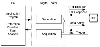
Now that we understand the architecture required to make synchronization happen, we must then look at methods to achieve synchronization in our application. The first method which is common with most basic synchronization tasks is to eliminate round trip delay (RTD) from the application. Take for instance the following application setup below:
Figure 2: Gen/Acq Synchronization Example Diagram - Stimulus Response
We can see that for stimulus/response applications, the time required for data to move from the digital tester, through the cable and DUT, and back to the tester can present a delay issue (RTD). The goal of this section is to provide a comprehensive, high-level overview of the tools we have available to compensate for this type of RTD; more details on each method can be found in the HSDIO help files, device specifications, or the many other HSDIO KnowledgeBase articles and whitepapers online.
A. DDC CLK OUT/STROBE, Data Active Event RTD Compensation
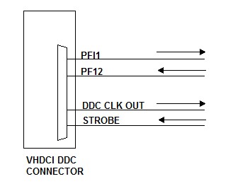
One way to do RTD compensation, and the method used in source-synchronous examples, is to export the sample clock/start trigger from the generation task, using DDC CLK OUT for the Sample Clock and PFI 1 for the Data Active Event (Start Trigger). The connections are then tied to the acquisition task via STROBE and PFI 2 input pins, respectively.
PFI1, PFI2, DDC CLK OUT, and STROBE are all on the DDC connector, and should be routed appropriately to the DUT via breakout board (such as the CB-2162) or with the flying lead cable.
The connections and process to program this procedure is demonstrated below:

Figure 3: Source Synchronous LabVIEW Example with Connection Diagram
Starting from the acquisition side, if we consider the diagram above for the 6556, the STROBE is routed through the same Digital Data and Control (DDC) connector as the rest of the Digital I/O (DIO) signals. From the Digital Waveform Generator/Analyzer Help:
“The advantage of using STROBE as the Sample clock source signal for the acquisition operation is that the acquisition session Sample clock and the data channels now travel together through the same cable and system delays, maintaining time correlation between them.”
For the generation task, the same process applies to the DDC CLK OUT line. Sending the clock signal along with the generation data ensures that the data channels have the same path delay as the clock signal internally to the HSDIO device. DDC CLK OUT is sent out synchronous with the data, so you are guaranteed to have data transitions occur at the clock transition points you have selected.
The Data Active event acts as the trigger for the acquisition and, since it is matched with the data, asserts at the right moment for acquisition to begin on the first sample correctly. A separate external connection does not have be made for the event since it resides in the DDC connector/cable path. In some situations, routing this signal out of PFI 0 may be necessary, which will require a different method for synchronization covered in the next section.
B. Other Methods for RTD Compensation
The method we described above is usually sufficient if the cables in use are length matched and the clock signal is able to be sent along the DDC connector. In the event that cables cannot be length matched, or a measurable delay is still noticed, there are a few other methods for RTD compensation. To use these methods, we must first know the total round trip delay, and figure out the number of clock cycles/fractional clock cycles of our generation clock this will take.
i. Data Delay/Data Position
Data Delay can be used to adjust the setup/hold time required for the application to improve the bit error rate (BER) of the application. Data delay is commonly used in synchronization applications.
Note: For details on delay resolution and allowed frequencies for each device, refer to the article on Advanced Features of High-Speed Digital I/O devices: Data Delay, or to the specifications manual for your device.
Data Position allows you to select rising edge or falling edge as the normal mode of sampling on your sample clock. This is commonly used to coarse adjust the data delay of a generation/acquisition. A great tip to use when building your application: set up the generation task for rising edge and the acquIsition task for falling edge data position. This means you will transition your generated samples on the rising edge, while sampling on the falling edge of the clock (presumably halfway in between rising edges). This works for most application that are cable length matched.
Note: For details on data positioning for each device, refer to the specifications manual for your device for a more detailed explanation and timing diagrams for generation/acquisition.
ii. Data Deskew (only supported on 6555/6556)
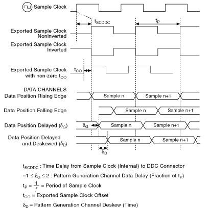
The Data Deskew property allows us to set the timing delay after the Sample clock edge when the device generates or acquires a new sample. This is applied independently of Data Delay, although it is the same circuit that performs the delay. The valid values, given in seconds, range between -2 to 3 sample clock cycles for both the 6555/56. The total combined delay from Delay and Deskew cannot exceed the range above. The idea behind Data Deskew is that the Deskew property can be used to cover any cable propagation delays measured, and the Data Delay property can be used for fine-tuned eye diagram and setup/hold time adjustments.
ViStatus = niHSDIO_SetAttributeViReal64 ( vi, channelName, NIHSDIO_ATTR_DATA_DESKEW, ValueOfDeskewInSeconds);
Figure 4: Data Deskew as Programmed in LabVIEW and C
An example of using Data Deskew properly would be when your test setup has to change its cabling requirements, but still stays the same in software. The new cabling will have a different propagation delay, which can be adjusted by the Data Deskew value. Setup and hold timing will therefore stay the same, making it easier to use when changing cables and/or applications.
iii. Internal Route Delay (IRD)
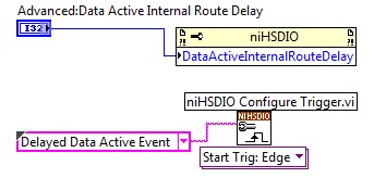
The Internal Route Delay property is a ‘coarse’ option that can be used for delay compensation when the Strobe/DDC CLK Out connections are not used. Setting this property allows us to delay the Data Active Event coming from our generation task by an integer number of clock cycles (refer to device specifications for valid values). Note that this property is only applicable in the acquisition session, and cannot be used in conjunction with the STROBE external clock source. The Data Active event will be automatically routed internally, so no routing configuration is necessary. However, the niHSDIO Configure Trigger VI on the acquisition should have the source parameter set to ‘Delayed Data Active Event’.
ViStatus = niHSDIO_SetAttributeViInt32 ( vi, channelName, NIHSDIO_ATTR_DATA_ACTIVE_INTERNAL_ROUTE_DELAY, ValueOfRouteDelayInSampleClockCycles);
Figure 5: Delayed Data Active Event and Internal Route Delay as Programmed in LabVIEW and C
iv. Sample Clock Offset
One final method for delay compensation that can be used in source-synchronous applications is the Exported Sample Clock Offset property. The exported generation sample clock will be delayed by a fixed time amount that varies depending on device.
ViStatus = niHSDIO_SetAttributeViReal64 ( vi, channelName, NIHSDIO_ATTR_EXPORTED_SAMPLE_CLOCK_OFFSET, ValueOfClockOffsetInSeconds);
Figure 6: Exported Sample Clock Offset as Programmed in LabVIEW and C
The following timing diagram should help to visualize how each of these properties will affect the data and clock positions of a generation session:
Figure 7: Clock and Data Position Timing Diagram
Note: more timing diagrams may be found in your device’s specifications manual.
Troubleshooting/FAQ
This section is intended to provide common tips and tricks for getting your synchronization of your HSDIO timing engines to work correctly.
A. Wrapback Synchronization
A possible first measure of success for using the HSDIO board with a DUT synchronously is to experiment by synchronizing the HSDIO board to itself. This requires making connections between the input and output of the board, the DDC CLK OUT connected to STROBE, and Data Active Event tied to the PFI trigger input terminal you have selected. Generate a ramp pattern and make sure it is acquired as expected on the HSDIO board. Once this is done, connect the board to the DUT and readjust the connections to test and see if synchronization is successful in your actual application.
B. Off by one
A common issue found in synchronization is sending your generated data to the DUT and then receiving it back ±1 sample off of what is expected. When this occurs, some suggestions are:
- Set Generation to generate off rising edge of sample clock, and set Acquisition to sample off the falling edge of sample clock by configuring Data Position for each session. This ensures you are not seeing jitter that could occur when you generate and acquire on the same edge.
- Use Data Delay to bring your acquisition sampling within setup/hold time.
- Verify matched trace lengths for your clocking, data, and trigger/event signals.
C. Common clocking errors
When using DDC CLK OUT/STROBE, clocking should be taken care of and delay should be compensated for in the clocking domain. However, there are times when this cannot be used, and CLK IN/CLK OUT SMB/SMA connectors are required, or potentially no clock at all. In these cases, propagation delay will cause significant differences in the timing of when you receive data based on when it is generated. Here are some common tips to minimize the impact of this setup:
- Use the internal route delay property to delay Data Active Event internal to your board and manually sweep/adjust the rate to have 0 percent bit errors.
- Match the SMA cabling as closely as you can to the data paths to mimic path delay.
- Use reference clocks to keep clock phases locked.
D. Signal integrity
Sometimes the signal coming from the DUT may be noisy, which causes bit errors despite synchronization. Carefully consider the proper cabling techniques and specifications of the system to achieve optimal signal integrity for your application.
