NI does not actively maintain this document.
This content provides support for older products and technology, so you may notice outdated links or obsolete information about operating systems or other relevant products.
Low Voltage Differential Signaling (LVDS) is an emerging differential digital standard used in several communication and mixed-signal applications. The electrical characteristics of an LVDS signal can facilitate significant performance improvements compared to single-ended standards. For example, since the received voltage is a differential between two signals, the voltage difference between the logic high level and low level state can be small, allowing for faster rise and fall times.
Another unique characteristic of LVDS is that it is a current-driven technology. Therefore, you must ensure your application has the correct termination and current-return paths.
Figure 1 shows a simplified diagram of a typical LVDS driver and receiver.
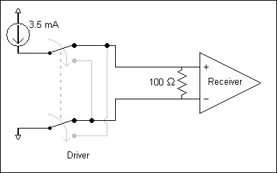
A current source at the driver provides approximately 3.5 mA of current. The direction of the current across the transmission line depends on whether the driver is driving a logic high level or low level. When the current reaches the receiver, a 100 Ω terminating resistor connects the two ends of the transmission line to provide a return path for the current. In addition, a voltage of approximately 350 mV is established across the two input terminals of the differential receiver. This differential voltage is either positive or negative, depending on the direction of the current. Based on the polarity of the voltage, the receiver recognizes the signal as either a high or low level.
As discussed in the introduction, LVDS is a differential, current-driven technology. The 655X, on the other hand, is a single-ended, voltage-driven digital waveform generator and analyzer. However, the flexibility of the 655X family of products allows you to easily interact with LVDS devices.
You can easily generate LVDS signals using two DIO channels to generate the two ends of the differential signal. The 655X devices have a 50 Ω source impedance on their output terminals that must be considered when configuring the voltage levels of a generation operation.
The full circuit, including an LVDS receiver, is shown in Figure 2.
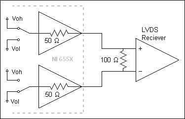
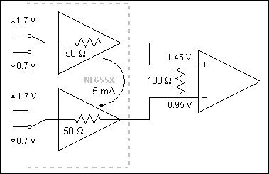
The NI 655X generation voltage levels must be set so that the appropriate current and voltage are seen at the receiver. Setting the generation voltage high level and generation voltage low level to 1.7 V and 0.7 V, respectively, works well. Those settings cause 5 mA to flow through the circuit, causing a voltage of 500 mV at the receiver (see Figure 3).
The LVDS specification allows for an input voltage range from 0 to 2.4V, so a wide range of acceptable values are available. The common-mode voltage seen at the receiver in this case is 1.2 V, which is within the ideal range for LVDS.
Figure 3 shows the current and voltage of the NI 655X LVDS circuit.
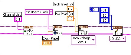
Programming the 655X to perform this generation is similar to programming a regular single-ended operation. As shown in figure 4, two channels are configured for generation. After you set the clock rate, set the voltage levels to the appropriate values, and then the device downloads the waveform. Notice that the data for the two channels are always inverse of one another.
Figure 4 shows the LabVIEW code snippet for programming a generation operation.
Another product, the NI 5421 is also capable of generating 16 channels of LVDS output. Either of the two higher memory options of the 5421 have this capability. See NI 5421 link at the bottom of this page for more information.
Like the generation method discussed above, the method for receiving LVDS signals with the NI 655X requires only a few special settings.
For an example of what happens if the correct settings are not used, assume both ends of an LVDS signal were wired directly to two input terminals on the NI 655X, each with 50 Ω input impedance. The circuit would look like Figure 5.
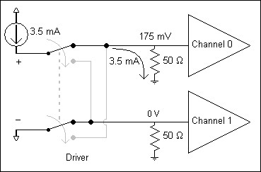
In this example, the driver’s constant current source attempts to push 3.5 mA through the positive wire. With a 50 Ω terminating resistor to ground, the voltage at the receiver is 175 mV, well below the desired LVDS common-mode voltage of 1.2 V. The negative leg is pulled to ground by the other 50 Ω resistor, forcing the voltage to be 0 V. Many LVDS drivers consider this to be an “open-fault” condition and stop functioning. You must change the circuit to prevent this open-fault condition.
Correcting the circuit requires you to complete the following two steps:
Keep in mind that the NI 655X can simultaneously acquire a dynamic signal and generate a static voltage on the same channel. After you complete these steps, the channel electronics for each channel look like Figure 6.
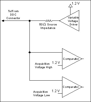
The variable voltage driver places 1.2 V on the output. If two such channels are combined with an LVDS driver, Figure 5 becomes the circuit shown in Figure 7.
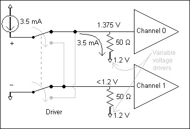
The two terminating resistors are both connected to 1.2 V, providing a complete current path with appropriate voltages. Depending on the LVDS device that you use, some current may be drawn through the negative leg of the signal, so the resulting voltage on channel 1 will be less than 1.2 V. The driver also inverts the signal, causing channel 0 to see the lower voltage (figure 8).
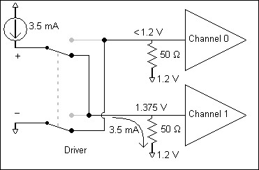
In this way, the voltage at channel 0 can toggle between 1.375 V and some voltage less than 1.2 V. Since the acquisition voltages on the NI 655X were set to 1.2 V, the comparators can detect these voltage changes, thereby reporting the correct sequence of 1’s and 0’s.
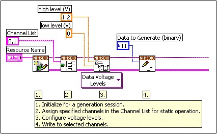
Creating this configuration requires only a small modification to a regular acquisition program. The LabVIEW code in Figure 9 initializes a generation session, assigns channels 0 and 1 as static generation channels, and sets one of the generation voltages to 1.2 V. The high-level voltage was used in this case, but either level may be used. Finally, the corresponding logic state is written to both of the channels, placing 1.2 V at the output of the variable voltage drivers for both channels.
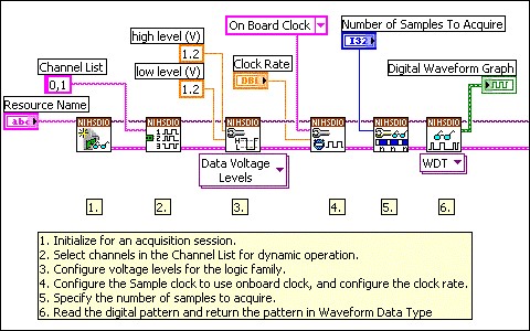
To acquire the signal, set up a normal acquisition. The only necessary change is to the acquisition high and low voltage settings. As mentioned earlier, NI recommends you set both acquisition voltage levels to 1.2 V, as shown in Figure 10.
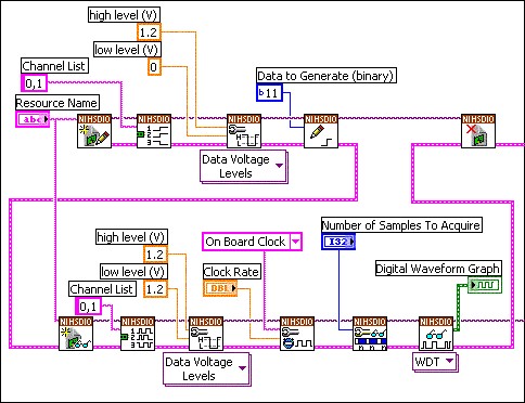
Combining the dynamic acquisition and static generation programs into a single VI is simple. Just ensure that the static voltage being generated on the channels is not cleared until after the acquisition has finished. To do this, wire the error cluster so that you ensure the proper order of execution. Do not close the generation session until after the acquisition is complete. Figure 11 shows one possible configuration for a combination VI.
So far, this application note has only addressed how to pass data back and forth between the NI 655X and the LVDS device. Frequently, however, an LVDS Sample clock signal must be passed between the two devices.
Exporting the Sample Clock
The easiest way to export a clock signal from the NI 655X is to simulate the clock with two DIO channels. Since the maximum Sample clock rate is 100 MHz (for the NI 6552), the maximum clock rate of a generated signal is 50 MHz. If a higher clock rate is desired, the true Sample clock can be exported using the DDC CLK OUT connector. The clock can also be exported using the SMB CLK OUT connector, but NI does not recommend using that connector for this operation.
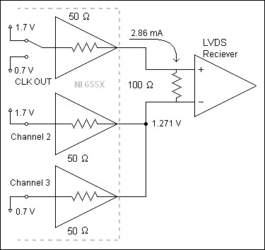
Ideally, a DIO channel can drive a static mid-point voltage to complete the current-return path. However, both generation levels are already being used as the high and low levels for the Sample clock. As an alternative, configure two static DIO channels to generate opposite voltages and short them together. The intersection of those two channels remains at a voltage that is near the midpoint, though the voltage fluctuates slightly as the sample clock toggles. An example circuit is shown in Figure 12.
Importing the Sample Clock
The acquisition method discussed above relies on the output drivers that exist on every NI 655X DIO channel. A Sample clock may be imported using the CLK IN connector or the STROBE channel (STROBE is only supported for acquisition sessions). Since CLK IN and STROBE do not have output drivers, you must use a different method to import a Sample clock.
First, choose either leg of the LVDS clock and connect it to the CLK IN SMB connector on the NI 655X device front panel. Unlike other channels, CLK IN is AC coupled with a default input impedance of 50 Ω to ground (as shown in Figure 13). The AC coupling allows the CLK IN terminal to detect the clock signal while still allowing a desirable common-mode voltage at the driver’s terminal.
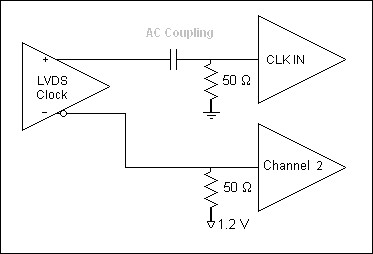
Another DIO channel (channel 2 in this example) must be used to complete the current path. To implement this circuit while acquiring data, modify the code shown in Figure 11 to change the Sample clock source to CLK IN and to add channel 2 to the static generation session. The resulting code is shown in Figure 14.
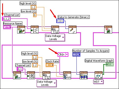
Notice that this acquisition method cannot be combined with the generation method discussed earlier in this application note. All generation channels (both static and dynamic) use the same high and low voltage levels. The generation method requires 1.7 and 0.7 V, while the acquisition method requires one of the levels to be 1.2 V. Therefore, if both acquisition and generation are desired, you must switch between the two operations, changing the voltage level settings between each operation.
Using the methods in this document, you can easily interface with an LVDS device using an NI 655X Digital Waveform Generator/Analyzer. NI has successfully tested these methods with the DS90LV027A from National Semiconductor, and other devices should work equally well.