Next-Generation Display with High-Throughput MiniLED Test
Yu-Min Hung, R&D Division Vice President, FitTech
Case Study Highlights
- FitTech significantly reduced physical space, test time, and increased scale to more channels than most of the SMUs on the market.
- NI’s PXI SMU helped improved steady-state response time, voltage boost, accuracy, stability, repeatability, reproductivity, responsivity, and resolution.
- FitTech decreased cost per channel and integration time while achieving higher quality test data.

“With hundreds of thousands Mini LEDs on a wafer, NI’s PXI-based high channel count SMU system with FitTech’s optical technology, provided us with highly accurate and repeatable measurements in smaller form factor than most solutions on the market today.”
—Yu-Min Hung, R&D Division Vice President
The Challenge
As LED chip sizes get smaller, the number of chips per wafer will increase to millions and tens of millions. The increased number of devices makes mass testing extremely difficult—increasing cost and test times from hours to days with current LED test solutions. FitTech needed to increase testing efficiency while still ensuring test stability and accuracy while testing miniLEDs.
The Solution
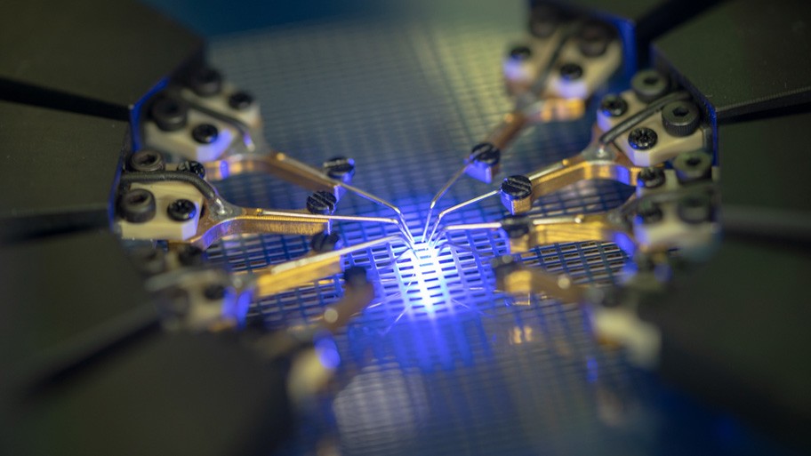
FitTech combined an in-house developed probing system, optical measurement system, and an electric measurement system using NI’s PXI Source Measure Units (SMUs) to quadruple throughput at eight LEDs at the same time, while still providing stable, efficient, and high-quality test results.
When Traditional Testing Solutions Can’t Keep Up
MiniLEDs and microLEDs are core light emitting technologies for the next generation of displays. As the LED chip size is miniaturized, the number of chips per wafer will increase from thousands to millions and tens of millions. The increased number of devices makes mass testing extremely difficult. The test time of each wafer will increase from hours to days if today’s LED test solutions are used. This bottleneck will be time-consuming and increase manufacturing costs. Significantly increasing testing efficiency while still ensuring test stability and accuracy is the main challenge of developing miniLED test solutions.
Leveraging the Benefits of Flexible Test Systems
We at FitTech are trying to solve this throughput challenge by testing faster and providing two systems in a single solution: an integrated LED prober and tester conducting optical and electrical measurements on each LED wafer. A typical LED testing machine is designed to test one or two chips at a time. But as LEDs shrink to hundreds of micrometers in size with miniLEDs, the number of chips per wafer dramatically increase: going from tens of thousands of traditional LEDs to hundreds of thousands of miniLEDs. Testing one or two LEDs at a time is just not fast enough to keep up with demand. To solve this challenge, we developed a parallel testing solution for miniLEDs. At FitTech, we combined this in-house developed probing system, optical measurement system, and an electric measurement system using NI’s PXI Source Measure Units (SMUs) to quadruple throughput at eight LEDs at the same time, while still providing stable, efficient, and high-quality test results.
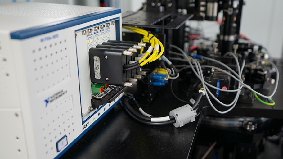
The NI SMU plays an important role in providing the right voltage and current setpoints for each LED and accurate measurement data. NI’s PXI SMU provides highly accurate and repeatable measurements that can provide four to eight channels in a smaller form factor than most SMUs on the market today, and NI can scale to meet hundreds of channels as LEDs get even smaller.
The Benefits of Implementing an Innovative NI Solution
We decided to use NI PXI-based SMUs for electrical test because they could save physical space, test time, and scale to more channels than most of the SMUs on the market today that only provide one to two channels with a similar footprint. With NI PXI SMUs, we can provide four to eight channels in a single chassis enabling parallel testing without increasing the test machine size.
In addition to footprint, we also saw faster test speed and higher-quality test data. Additionally, we improved steady-state response time, voltage boost, accuracy, stability, repeatability, reproductivity, responsivity, and resolution compared with our previous solution. Higher-resolution SMUs allowed us to provide higher accuracy testing to benefit our wafer manufacturers. Additionally, with the modular PXI-based architecture, we saw cost per channel decrease and integration time get faster.
The NI PXI SMU uses a PCI Express interface as opposed to the slower GPIB or Ethernet interfaces, which are more common on the market. NI PXI SMUs offer high-performance data transmission and capture, and improved synchronization to optical measurement systems as well as all electrical test channels, which is critical for parallel testing of miniLEDs.
Finally, with NI’s PXI SMUs built-in ADC converters, we drastically reduced our time to integrate multichannel data acquisition and perform high-frequency sampling, which are also important for preventing distortion and raising measurement accuracy. In addition to the built-in ADC, NI’s I/O Trace tool, which we could use for monitoring and recording, provided a more convenient way to analyze the test process and troubleshoot during integration.
Overall, developing a high-quality testing system for miniaturized chips with high stability, accuracy, and efficiency is quite a challenge. Using NI PXI SMU in the FitTech miniLED testing system not only provides flexibility and high performance, but also reduces the developing time and cost of integrating systems.
Results and Value
At FitTech, we pioneered and have been providing a combined LED probing and test solution for more than 17 years. Our customers can streamline support and test service with one company and by partnering with NI, we are now providing faster parallelized test capabilities—which means higher throughput with fewer test and probe machines. Parallel testing is a core concept of providing miniLED test solutions. On the one hand, we optimized our probe system with better stability, speed, and accuracy of motion; with our self-design Load Cell edge sensor, we provide fewer and identical needle marks. On the other hand, we use the NI PXI source measure unit in the test system, allowing us to successfully achieve parallel testing without increase machine physical volume. With these optimizations and usage of NI SMUs, we decreased our electronic test time by 30 percent and overall test time by 10 percent compared to our previous solutions.
Looking Ahead
As LEDs become even smaller, we will see a ramp in the usage of microLEDs (areas smaller than 50 microns). The number of chips on every wafer will dramatically increase. While the market is still new, and many manufacturing and test approaches are being considered, NI and FitTech are committed to providing the right instrumentation and test systems for efficient and accurate microLED test to provide the best yields for wafer manufacturers.


