Using Wideband IF Digitizers to Solve Challenges in Streaming and Recording RF Signals
Overview
Contents
- The Challenge
- Wideband Streaming
- Narrowband Streaming
- Phase Noise Considerations and Improvements
- Conclusion
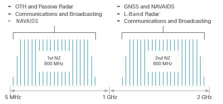
Figure 1. Example Signals in 5 MHz–2 GHz Band
The Challenge
Many applications in verification and validation tests, spectrum surveillance, multiconstellation GNSS, and software-defined receivers require acquisition, real-time processing, and recording of RF signals. Modern analog-to-digital converter (ADC) technology enables direct sampling receivers operating at or above 2 GHz. This simplifies the architecture of the receivers, mainly in the case of multichannel systems, which require tight synchronization between channels. That is the case in direction finding systems for spectrum surveillance, over-the-horizon and passive radar, and antenna measurements.
Furthermore, the increasing demand for faster spectrum scanning and new types of radar requires receivers with wide instantaneous bandwidth and real-time signal processing.
Normally, current RF streaming systems take two forms: high-bandwidth, lossless streaming and narrowband streaming. The first type records all available bandwidth, which in modern applications implies gigabytes per second of data for systems sampling at 2 GS/s or higher. Active radar systems typically take advantage of wideband streaming.
Often, however, most of the useful information concentrates around a particular narrower band. This is where the second type of streaming comes in. Narrowband streaming enables data reduction and inline signal processing. Such systems require streaming to HDD signals that occupy relatively narrow bands with several central frequencies.
Example narrowband signals acquired, streamed, and analyzed (or recorded) by passive radar applications can originate from Digital Video Broadcasting—Terrestrial (DVB-T) or Advanced Television Systems Committee (ATSC) transmitters that are characterized by bandwidths of 6 MHz to 8 MHz, depending on the country, and are in VHF/UHF frequency ranges.
GNSS multiconstellation receiver tests are other examples for narrowband streaming, where the requirement is to use both GPS L5/L2 and GLONASS G1 and G2 signals. Users might focus their interest in signals that are only a few megahertz wide but that can be spaced even hundreds of megahertz apart.
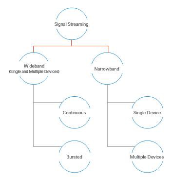
Figure 2. Classification of Streaming Applications Covered in This Document
After acquiring these wideband signals, these streaming systems require subsequent downconversion (shift in frequency), decimation, equalization, and calibration. The resulting narrowband signal then gets demodulated and decoded, further filtered, amplified, and stored to HDD or any combination of these functions.
At a high level, typical streaming and channelizing applications can be divided as figure 2 shows.
Wideband Streaming
To better understand the challenges connected with wideband streaming, one must first understand the technical specifications of the IF receiver. This paper focuses on the PXIe-5624R module. IF receivers are typically part of the vector signal analyzer that comprises the mixer, IF receiver, and signal sources for LO. The architecture of the example vector signal analyzer is described in the Introduction to the PXIe-5668R—High-Performance 26.5 GHz Wideband Signal Analyzer white paper.
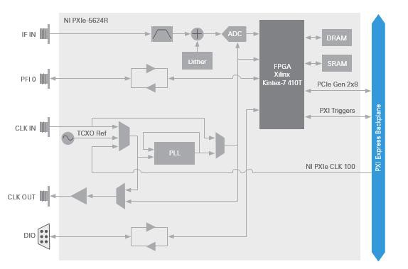
IF is characterized by the frequency range from 5 MHz to 2 GHz and bandwidth of 800 MHz typical (see technical specs for details). After adding a band-limited noise (dither) signal, which helps reduce the quantization effects of the ADC and improve spectral performance, the ADC samples the signal at up to 2 GSa/s with 12-bit resolution. The onboard FPGA processes these samples and transfers the data to other devices (PXI Express controller, RAID) through the PCI Express Gen 2x8, which allows for data streaming with theoretical rates of up to 4 GB/s. In the wideband streaming case, the FPGA performs only one digital downconversion (DDC) for all incoming data, as opposed to several independent downconversions in the narrowband case as mentioned later in the document.
Figure 3. Block Diagram of the PXIe-5624R IF Digitizer
Bit Packing
When talking about wideband streaming, one must consider not only the theoretical available bandwidth of the PCI Express bus but also its practical limitations (that is, control messages that travel over the same bus). The first and more simple implementation for sending data over the PCI Express bus would be to send 16-bit samples, one after another, even if data from the ADC is only 12 bit. However, this approach leads to theoretical limitations of 4 GB/s per PCI Express link available in the PXIe-5624R module (2 bytes/samples at 2 GS/s equals to 4 GB/s), which practically won’t allow for continuous streaming. However, there’s a clever solution: bit packing. Using bit packing, four 12-bit samples are packed into three 16-bit words. Consequently, this method reduces the data rate from 4 GB/s to 3 GB/s, enabling continuous data streaming.
Intermodules Synchronization
Often there is a need for continuous streaming from several modules of the same type. These multichannel, synchronized RF systems enable certain applications such as direction finding. By analyzing the incoming signal’s phase difference between different channels, the system can determine the direction of the signal source.
In such case, the digitizers are locked to the same reference clock. By default, this is the 100 MHz PXI Express backplane clock. Therefore, the synchronization makes it possible to start the acquisition on multiple devices at the same time—more precisely, within a couple of 10 ps relative to each other. But, it is critical that the skew between the digitizers is the same from run to run as long as the temperature is the same, so the skew can be improved with calibration. No timing module or external cabling is required for the synchronization to work. The synchronization uses two trigger lines on the PXI Express backplane.
Burst Mode
In burst mode, the data is streamed to the host only after the trigger signal occurs. The trigger signal can be connected directly to the IF digitizer board using the PFI0 connector, or it can be software-triggered. In burst mode, users can define logic of the FPGA in a way that a few parameters can be configured:
- Record length (Nx)
- Record period (Mx)
- Number of records per trigger
- Number of pretrigger samples
Figure 4. Example Burst Acquisition Scenario
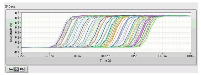
Such a burst scenario can be implemented in a way that allows for variable record lengths and delays. Descriptions of scenarios can be defined on the host machine and later streamed down to the FPGA. The trigger signal, however, can produce samples with an uncertainty of around 8 ns, because the PFI0 signal being sampled at 125 MHz.
Figure 5. Trigger Uncertainty Resulting From PFI0 Being Sampled at 125 MHz
Narrowband Streaming
Narrowband streaming is often needed in GNSS validation, spectrum monitoring, passive radar, and direction finding applications. In such cases, users often are interested in multiple relatively narrowband signals that are within a defined, larger spectrum component and often coming from multiple spatially distributed antennas.
The strong requirement is that the signals are acquired simultaneously, which makes it impossible to use traditional, swept vector signal analyzers. The solution for such a challenge is called a channelizer—the application that acquires a wideband signal containing all narrowband signals of interest and then separates them using DDC on an FPGA, thereby significantly reducing data rates.
Digital Downconversion
Because of its parallel structure, it is possible to implement numerous DDC logic blocks on an FPGA, allowing for the simultaneous analysis of multiple narrowband signals. The first stage of DDC uses a digital quadrature mixer that shifts a signal to baseband from any frequency within the range of the digitizer. The next stage decimates (reduces the sample rate). Programmable digital FIR lowpass filters prior to each stage of decimation prevent aliasing when the sample rate is reduced. Users can retrieve the decimated data as in-phase and quadrature.
Additionally, users can perform digital signal processing for the digital correction of analog imperfections in the system such as:
- Digital Gain—Digitally controls the I and Q signal amplitudes
- Digital Offset—Digitally controls the I and Q signal offsets
- Equalization—Filters the I/Q data to equalize the analog response of a device
- I/Q Impairments—Modifies the I/Q data to correct or apply I/Q impairments such as gain imbalance, quadrature skew, or DC offset
One PXIe-5624R device with its Xilinx Kintex-7 XC7K410T can fit up to 12 DDCs with 37.5 MHz I/Q rates or 8 DDCs with 93.75 MHz I/Q rate (contact NI for details). Subbands can be streamed to RAID and/or analyzed online on the host machine.
Multiantenna DDC Using IF Receivers
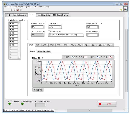
As mentioned above, multiple PXIe-5624R devices can be synchronized for acquisition from multiple antennas, for example, for direction finding applications. In such cases, users can define up to 12 center frequencies with selected I/Q rates and multiple IF modules will downconvert signals from multiple antennas. The PXI Express solution simplifies the synchronization of the multiple PXIe-5624R ADCs.
- The following parameters can be set in such case:
- Channels’ center frequencies
- Channels’ I/Q rate
- ADC clock source
- Clock out
- Burst size (for burst acquisition)
- Burst wait period in samples
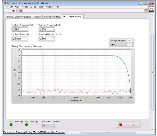
- Shaping filter’s parameter
Figure 6. Example Configuration Window for a Multimodule, Multichannel Channelizer Application
Figure 7. Shaping Filter’s Parameters
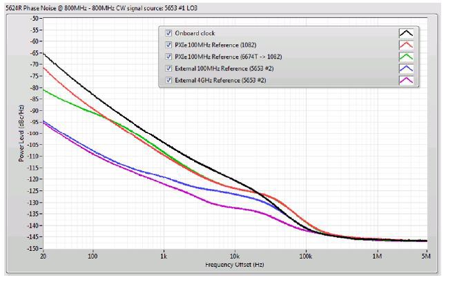
Figure 8. Various Options for Phase Noise Reduction
Phase Noise Considerations and Improvements
The open architecture of the PXIe-5624R IF receivers allows for using external clock signals in applications where keeping the phase noise to a minimum plays a critical role. Users can choose the best way of providing clocking signals to ADC, depending on the requirement of the system and available budget. Figure 8 shows various possible configurations of clock sourcing. The PXIe-6674T module is a timing and synchronization module developed for multimodule, multichassis systems (phase noise marked with green on Figure 8), whereas PXIe-5653 is a low-phase noise LOs generator (marked with blue and purple on Figure 8). Lowest phase noise is achieved with the PXIe-5653 module, whereas PXIe-6674T is a compromise between cost and performance.
Conclusion
NI’s PXI-based IF receivers (PXIe-5624R) with built-in FPGAs are powerful devices that empower some of the most demanding streaming applications such as radar test, GNSS validation, agile spectrum monitoring, and direction finding. Their open architecture in combination with the power of the PXI platform allow for easy expansion into multiple channels with guaranteed phase synchronization and coherence.
Furthermore, the NI modular approach allows users to add components such as mixers (with central frequencies up to 26.5 GHz in PXI Express form factor or 72 GHz to 76 GHz radio head), switches, power amplifiers/attenuators, and preselector modules.
