How Does NI USRP Hardware Work?
Overview
NI Ettus Universal Software Radio Peripheral (USRP) devices are software defined radios (SDR) used for wireless and RF applications. NI Ettus USRP transceivers can transmit and receive RF signals in several bands, and you can use them for applications in communications education and research. Paired with the LabVIEW development environment, USRPs provide an affordable solution that lets you validate wireless algorithms with over-the-air signals.
Contents
Software Defined Radio
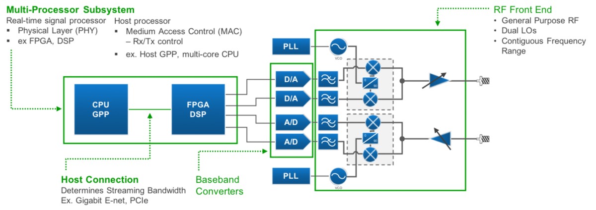
The SDR architecture typically includes processors—whether that is on board or the computer—FPGAs and tunable RF front ends. USRP and LabVIEW offer flexibility, functionality, and affordability to deliver an ideal SDR prototyping solution for educational laboratories and communications research.
Figure 1: Typical architecture of a software-defined radio
LabVIEW provides the signal processing engine for the modulation and demodulation of signals streaming to and from USRP hardware. You can add the LabVIEW Real-Time and LabVIEW FPGA modules to target NI Linux Real-Time OSs and FPGAs all from the same development environment. LabVIEW also offers functional blocks for many common analog and digital modulation techniques and signal processing algorithms optimized for real-world radio signals.
Common Applications
USRP hardware works with a wide range of applications. The flexibility and affordability of the hardware mean you can use the products from teaching to advanced wireless research, including dynamic spectrum access, whitespace, and PHY- and MAC-layer research. The products are also useful in simple transmit or receive applications for building custom protocols or logging spectrum to disk.
Hardware Overview
3a. Host-Only USRP
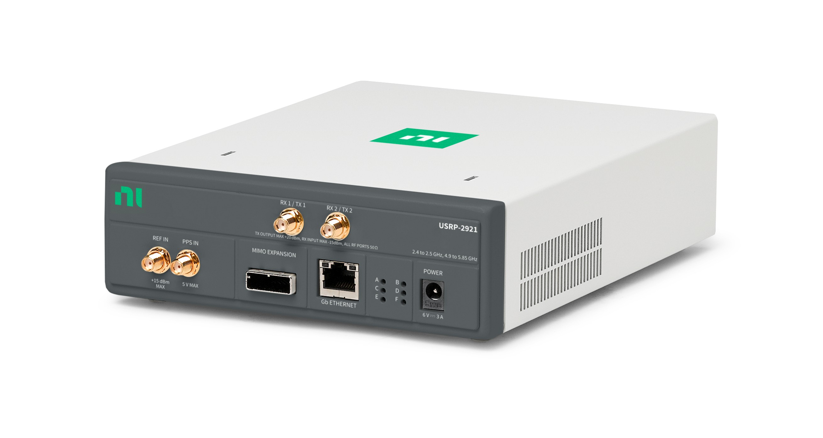
Figure 2: NI USRP-2921
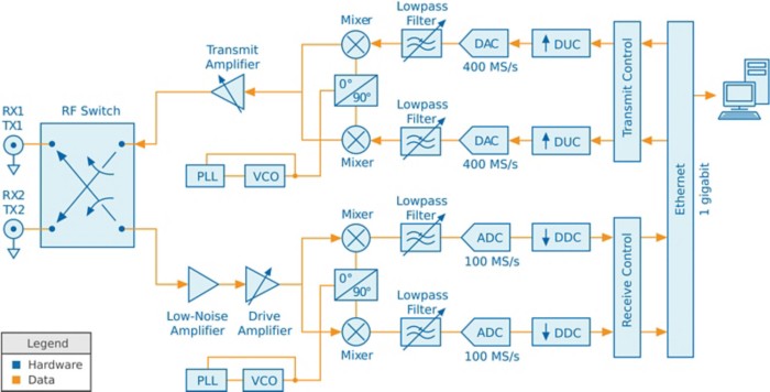
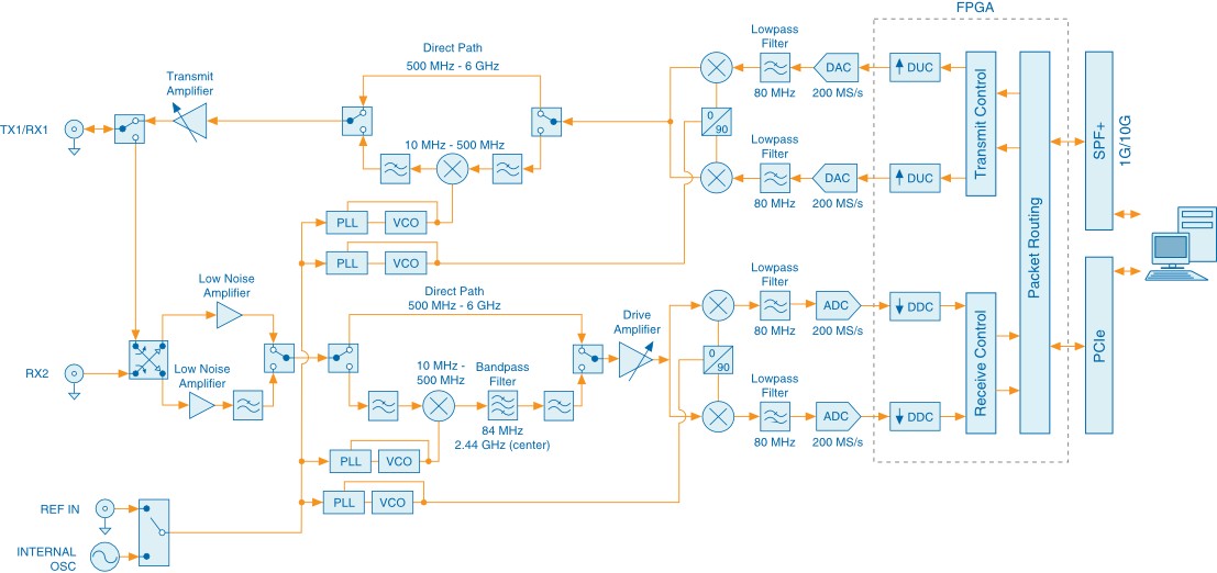
Following a common SDR architecture, USRP hardware implements a direct conversion analog front end with high-speed analog-to-digital converters (ADCs) and digital-to-analog converters (DACs) featuring a fixed-personality FPGA for the digital downconversion (DDC) and digital upconversion (DUC) steps. The receiver chain begins with a highly sensitive analog front end that can receive very small signals and digitize them using direct downconversion to in-phase (I) and quadrature (Q) baseband signals. Downconversion is followed by high-speed analog-to-digital conversion and a DDC that reduces the sampling rate and packetizes I and Q for transmission to a host computer using Gigabit Ethernet for further processing. The transmitter chain starts with the host computer where I and Q are generated and transferred over the Ethernet cable to the USRP hardware. A DUC prepares the signals for the DAC after which I-Q mixing occurs to directly upconvert the signals to produce an RF frequency signal, which is then amplified and transmitted.
Figure 3: USRP-2921 System-Level Diagram
3b. USRP Devices with Programmable FPGAs
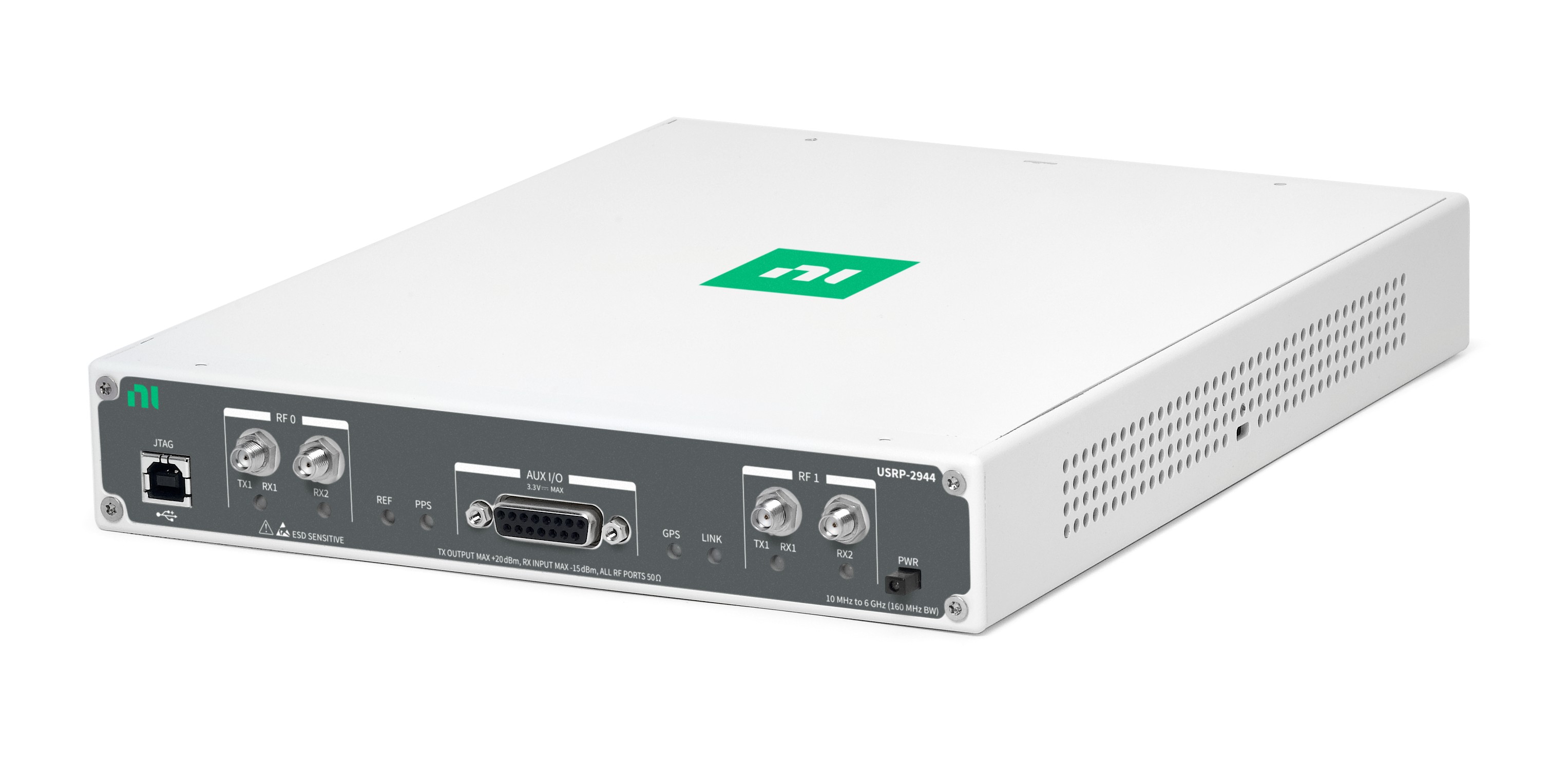
Figure 4: NI USRP-2944
The NI USRP-294x/295x devices combine two full-duplex transmit and receive channels with up to 160 MHz/channel of real-time bandwidth and a large DSP-oriented Kintex-7 FPGA in a half-1U rack-mountable form factor. The analog RF front end interfaces with the large Kintex-7 410T FPGA through dual ADCs and DACs clocked at 120 MS/s.
Each RF channel includes a switch allowing for time division duplex (TDD) operation on a single antenna using the TX 1 RX1 port, or frequency division duplex (FDD) operation using two ports, TX1 and RX2.
The NI USRP-294x/295x devices cover from 10 MHz to 6 GHz frequency range with user-programmable digital IO lines for controlling external devices. The Kintex-7 FPGA is a reconfigurable LabVIEW FPGA target that incorporates DSP48 coprocessing for high-rate, low-latency applications. The PCI Express x4 connection back to the system controller allows up to 800 MB/s of streaming data transfer back to your desktop or PXI chassis, and 200 MB/s to your laptop. This connection allows up to 17 USRP devices to be cabled back to a single PXI Express chassis, which can then be daisy chained together for high-bandwidth, high-channel-count applications.
Figure 5: USRP-2944 System-Level Diagram
3c. NI USRP-2974 Stand-Alone Device
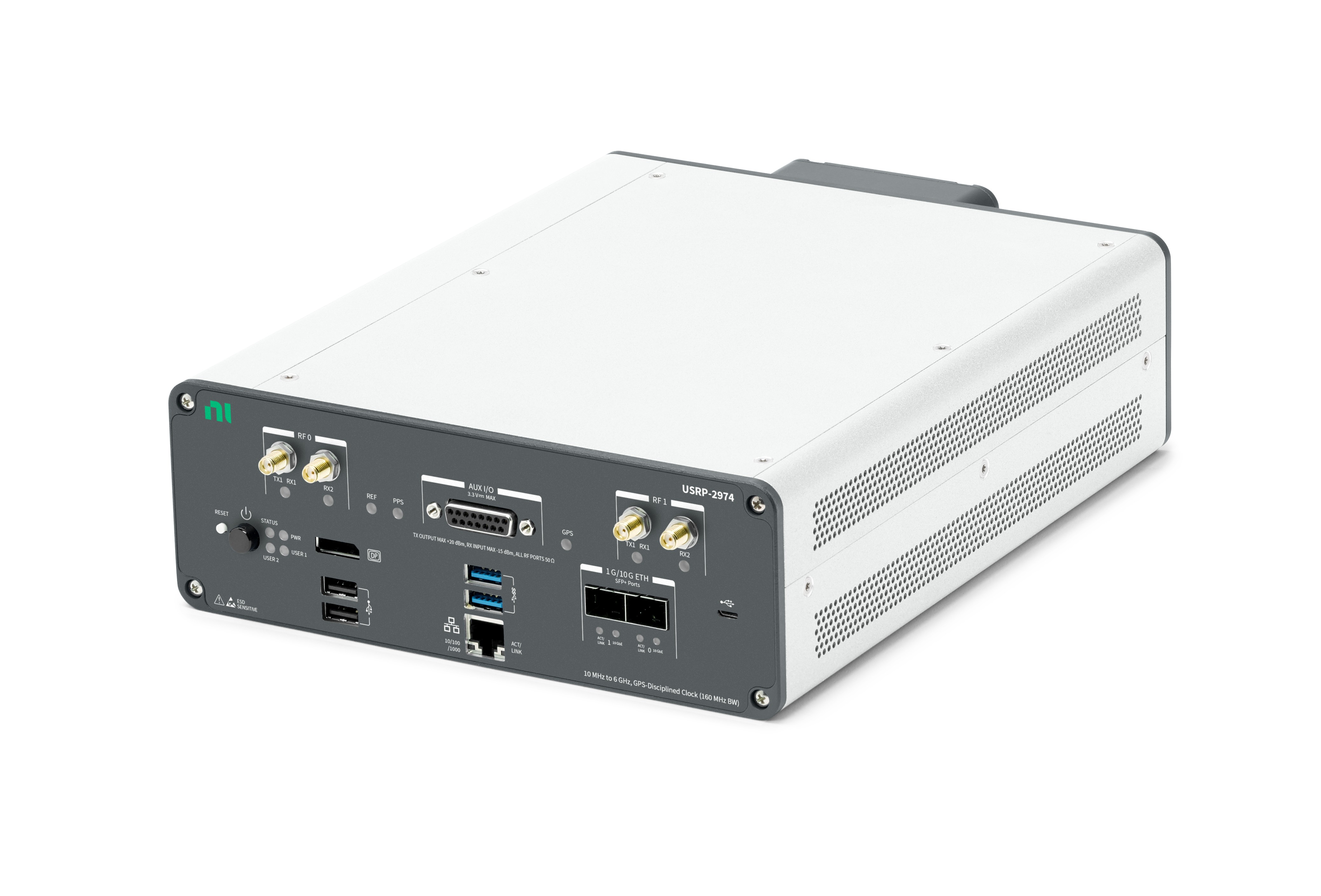
Figure 6: NI USRP-2974
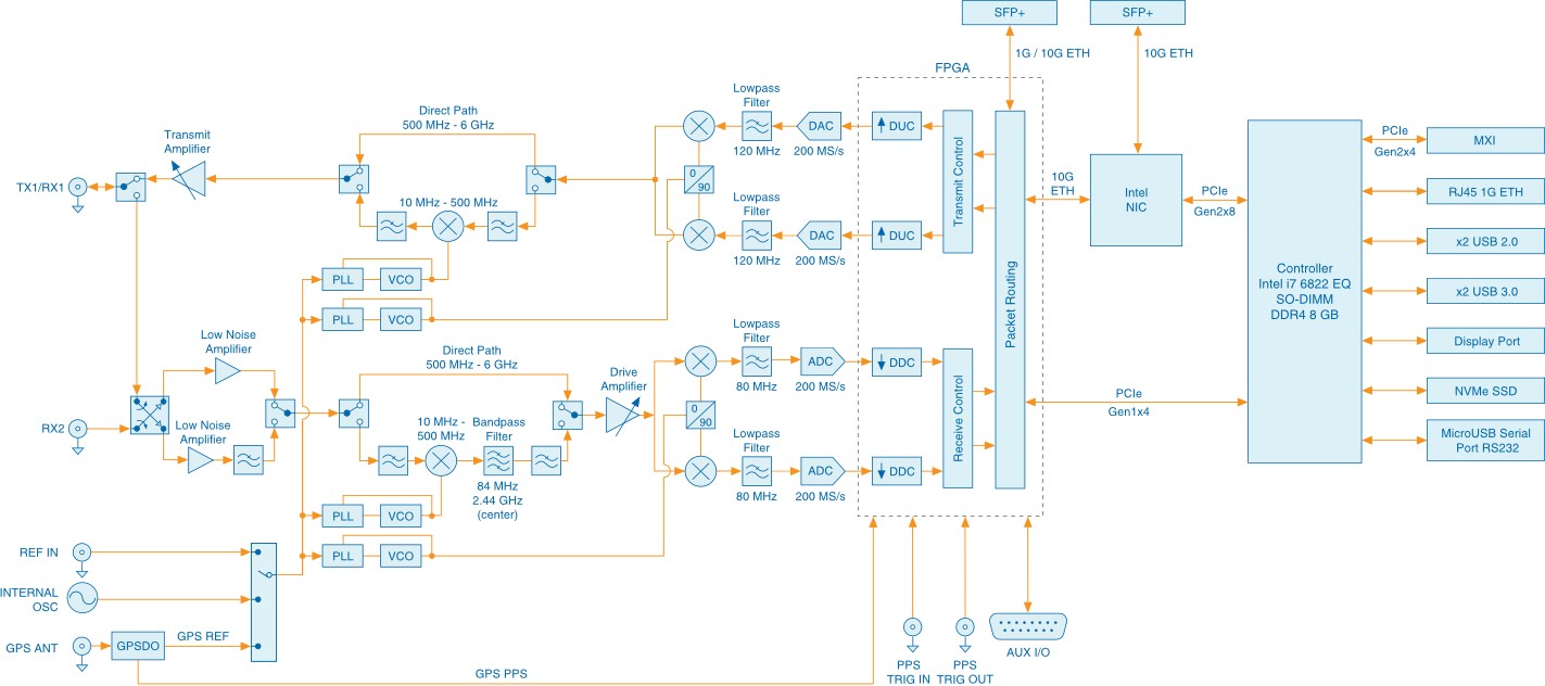
The stand-alone NI USRP-2974 includes an onboard processor, FPGA, and RF all in one form factor. The USRP-2974 is built on a heterogeneous processing architecture with an onboard Intel Core i7 processor running the NI Linux Real-Time OS. It is a 2x2 radio that covers frequencies between 10 MHz and 6 GHz with the 160 MHz bandwidth and adds an x86 processor to form stand-alone system operation, which can be targeted to deterministically perform processing and program the Xilinx Kintex 470 FPGA all from a single design environment. The USRP-2974 is also equipped with a GPS-disciplined 10 MHz oven-controlled crystal oscillator (OCXO) Reference Clock.
Figure 7: USRP-2974 System-Level Diagram
Software Overview
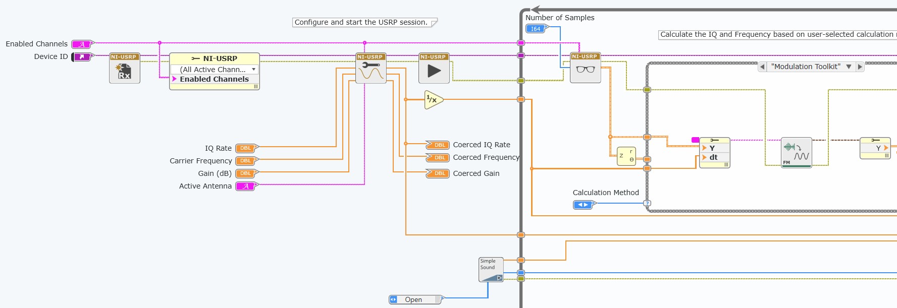
LabVIEW is a graphical dataflow programming environment well suited for designing and implementing communications algorithms. At the most fundamental level, LabVIEW uses the NI-USRP driver to both specify USRP hardware configuration and send and receive properly formatted baseband I/Q data.
Figure 8: Screenshot of a LabVIEW block diagram with the USRP driver API
Next Steps
- View all NI USRP products
- Learn which USRP is right for you
- Learn how USRP is advancing wireless prototyping
The registered trademark Linux® is used pursuant to a sublicense from LMI, the exclusive licensee of Linus Torvalds, owner of the mark on a worldwide basis. MATLAB® is a registered trademark of The MathWorks, Inc.
