Overview of the NI USRP RIO Software Defined Radio
Overview
The NI USRP RIO is an SDR game changer that provides wireless communications designers an affordable SDR with unprecedented performance for developing next generation 5G wireless communication systems. "USRP RIO" is a term that is used to describe USRP Software Defined Radio Devices that contain an FPGA, such as the USRP-294x and USRP-295x. These devices have a state-of-the-art 2x2 MIMO RF transceiver with a LabVIEW programmable DSP oriented Kintex 7 FPGA. LabVIEW provides a unified design flow that enables wireless communications researchers to prototype faster and significantly shorten time to results. The NI USRP RIO extends the USRP platform with a refined user experience making SDR prototyping more accessible by delivering the optimum balance of performance and streamlined software tool flow. It is ideal for a wide range of application areas that include 5G wireless communications, massive MIMO , spectral monitoring, and many more.
Contents
- USRP RIO Architecture
- Optimized RF Performance
- Timing and Clock Distribution
- Connectivity Options
- NI USRP Software Drivers
- Code Sharing Community
- Watch a Demonstration of the USRP RIO Software Defined Radio
USRP RIO Architecture
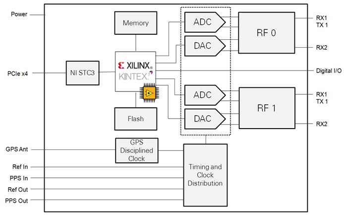
The NI USRP RIO software defined radio platform combines two full-duplex transmit and receive channels with 40 MHz/channel of real-time bandwidth and a large DSP oriented Kintex 7 FPGA in a half-1U rack mountable form factor. The analog RF front end interfaces with the large Kintex 7 410T FPGA through dual ADCs and DACs clocked at 120 MS/s.
Each RF channel includes a switch allowing for time division duplex (TDD) operation on a single antenna using the TX 1 RX1 port, or frequency division duplex (FDD) operation using two ports, TX1 and RX2.
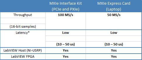
USRP RIO devices have frequency options that span from 50 MHz to 6 GHz with user programmable digital IO lines for controlling external devices. The Kintex 7 FPGA is a reconfigurable LabVIEW FPGA target that incorporates DSP48 co-processing for high-rate, low latency applications. PCIe Express x4 connection back to the system controller allows up to 800 MB/s of streaming data transfer back to your desktop or PXI chassis, and 200 MB/s to your laptop. This connection allows up to 17 USRP RIO devices to be cabled back to a single PXI Express chassis, which can then be daisy-chained together for high-bandwidth, high-channel-count applications.
Figure 1. USRP RIO System Block Diagram
Optimized RF Performance
The USRP RIO RF performance is characterized at the time of manufacturing, and correction factors are written to the device EEPROM to compensate for I/Q imbalance, DC offset, and absolute accuracy. These correction factors are loaded and digitally applied to the baseband I/Q data by the FPGA only when using the LabVIEW FPGA sample streaming project and derived projects.
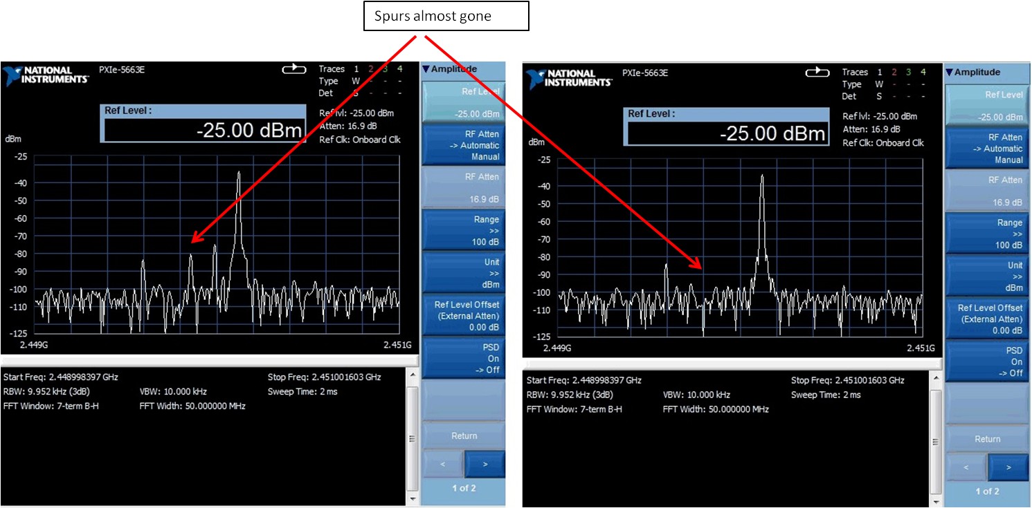
The outcome of applying these corrections is a significant improvement on the LO and image spurs whether the device is transmitting or receiving signals, and an absolute power level accuracy of ±3 dB over the device operating frequency range.
Figure 2. shows the noncorrected vs corrected performance of the USRP-2953 transmitter at 2.45 GHz. With corrections, the LO and image spurs are almost gone.
Figure 3. shows a ~17 dB improvement on the LO and image spurs for a received signal on the USRP-2953.
Figure 2. Noncorrected versus Corrected TX Performance at 2.45 GHz
Figure 3. Noncorrected versus Corrected RX Performance at 2.45 GHz
Timing and Clock Distribution
The USRP-294xR devices include a TCXO (temperature controlled oscillator) as the base frequency reference, which works well as a general purpose oscillator. The USRP-295x devices include a precision GPS-Disciplined OCXO (GPSDO), which provides improved frequency accuracy without using GPS and significantly improves frequency accuracy when disciplined to the GPS satellite network.
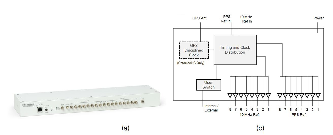
All USRP RIO models include options for using an internal or external clock reference with the added ability to export the clock reference and time base. The Ref In port accepts a 10 MHz reference from which the ADC/DAC clocks and local oscillator are derived. PPS In can be used as a standard pulse per second port or as a general-purpose digital trigger input line. Ref Out and PPS Out allow either of those signals to be exported for building higher channel count systems. Amplified clock distribution, using the 8 channel OctoClock and the NI PXIe-6674T, allows users to build extremely large synchronized systems by connecting it to the Ref In and PPS Using several Octoclocks, you can build systems that exceed 100 synchronized channels.
Figure 4. OctoClock-G Module (a) and System Diagram (b)
Connectivity Options
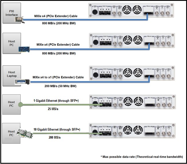
The primary bus interface for the USRP RIO is PCIe x4, which provides an effective connection for high-bandwidth and lower latency applications such as PHY/MAC research. The bus allows users to stream data at 800 MB/s and customize the FPGA in LabVIEW FPGA. The interface is backwards-compatible with programs written for the USRP-292x and USRP-293x devices. The USRP-294x/295x devices with the NI-USRP driver in LabVIEW also support connectivity over 1G and 10G Ethernet using the SFP+ ports on the back of the device; however, you cannot modify the FPGA when connected over Ethernet.
Figure 5. USRP RIO Interface Options
Figure 5. shows the available interface options that allow users to the USRP RIO to a laptop, desktop PC, or rugged PXI chassis. When connected to a PXI chassis, multiple USRP RIO devices can share data through the backplane of the PXI chassis without having to go through the host, using peer-to-peer streaming (P2P).
Table 1. Performance for the Different Connectivity Kits
NI USRP Software Drivers
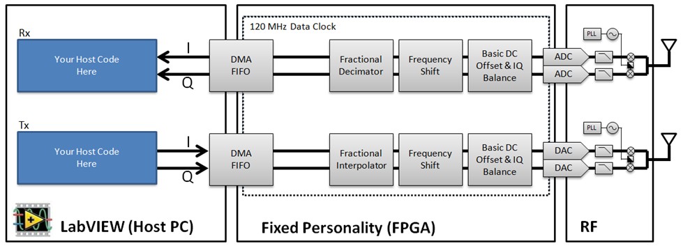
NI USRP RIO utilizes two complementary LabVIEW based software driver experiences: a host based driver (NI-USRP), and a fully open and customizable LabVIEW FPGA experience (NI-USRP RIO). Both driver interfaces support connectivity over PCI Express and use a similar driver approach allowing users to efficiently take their design from the host computer to the FPGA. NI-USRP also supports connection over 1G or 10G Ethernet for USRP-294x/295x devices, but using LabVIEW FPGA is not supported in this configuration.
NI-USRP Driver
NI USRP RIO releases with NI-USRP 14.0 driver support and later provide a seamless host-based interface that is fully backward-compatible with USRP-292x and USRP-293x devices. Using a fixed FPGA image configurable from the host API allows users to develop their algorithm in LabVIEW and seamlessly move between NI USRP and NI USRP RIO devices.
Figure 6. Typical Streaming Application Using NI-USRP driver (Host Only)
NI-USRP RIO Driver
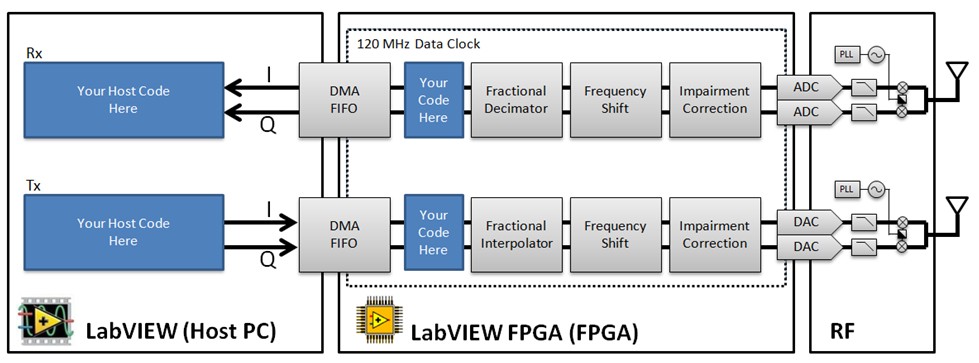
As applications require increased performance, users can utilize the large Kintex 7 FPGA for co-processing by migrating their design using the NI USRP-RIO driver. The NI USRP RIO driver provides a streaming sample project that includes open host processor and FPGA design code written in LabVIEW and LabVIEW FPGA respectively. The sample project can be configured so that the code runs only on the host, and/or modify the FPGA personality to include custom processing. While the entire FPGA reference design is customizable, will most often insert their code in the signal chain near the DMA FIFO. The streaming sample project is based on the “Instrument Design Library” reference design common to NI FlexRIO SDR and the NI Vector Signal Transceiver (VST).
Figure 7. Typical Streaming Application using NI-USRP RIO driver (Host and FPGA)
Code Sharing Community
Support for the NI-USRP driver also enables reuse of code housed in the USRP code sharing community. Examples include a FM radio, decoding ADS-B passive radar signals, capturing 802.11b SSID, and more.
Watch a Demonstration of the USRP RIO Software Defined Radio
