Understanding the SPI Bus with NI LabVIEW
Overview
Contents
- SPI Bus Overview
- Basic Connections
- Basic Transmission Step-by-Step
- Parameters of the SPI Protocol
- SPI Timing Considerations
- Strengths and Weaknesses of SPI
- Browse, Download and Share SPI Device Drivers and FPGA IP
SPI Bus Overview
The SPI serial bus was originally established by Motorola. Today, it is one of the most common communication buses used by integrated circuit manufactures for device to processor or FPGA control. Examples include ADCs, DACs, sensors, and board-only products. Although it is not regulated as a standard by IEEE or another organization, most devices adhere to common set of rules described in this document.
SPI is a synchronous serial data link that operates in full duplex. That is, signals carrying data go in both directions simultaneously. Devices communicate using a master/slave protocol, in which the master starts the data frame. When the master generates a clock then selects a slave device, data may be transferred in either or both directions simultaneously. It is up to the master and slave devices to know whether a received byte is meaningful. This may require a device to discard the received byte in a "transmit only" frame or generate a dummy byte for a "receive only" frame.
Basic Connections
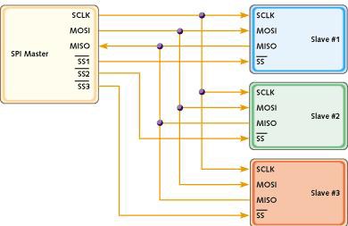
The four typical SPI signals include:
- clock (SCLK) - This signal is generated by the Master. Other signals in the transmission change based on the timing of edges from this clock.
- master data output, slave data input (MOSI) - This line is the output from the Master to the slave. Transmits bit-by-bit synchronized with Master clock edges.
- master data input, slave data output (MISO) - This line is the output from all the slaves connected. Transmits bit-by-bit from the slave synchronized with Master clock edges.
- chip select (CS) or slave select (SS) - This is a bank of signals where each line goes to individual slaves in the system. One line is asserted at a time to enable communicate with the corresponding slave. Chip select is commonly asserted low.
Figure 1: Master connected to one slave.
Figure 2: Master connected to multiple slaves. Notice the bank of Chip select lines connected to the individual slaves to enable communication with one at a time.
Basic Transmission Step-by-Step
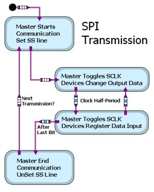
- The Master drives a particular SS line low to initiate communication with the corresponding slave.
- Once the selected SS is low, one edge (rising or falling) of the SCLK signals the devices (Master and Slave) to toggle the MOSI and MISO to the correct bit of data being transmitted.
- The other edge of the SCLK line (rising or falling) signals the devices to register the bits on the MOSI and MISO, effectively reading the bit into the device.
- The transmission continues in this fashion until the devices have exchanged the specified number of bits (usually 8,16, or 32)
- After the transmission is complete the Master pulls the SS line for the slave back high and either goes to another slave on the network or reinitiates the transmission with the same slave by pulling the corresponding SS line back to low.
Figure 3: Statechart of the basic SPI transmission
Parameters of the SPI Protocol
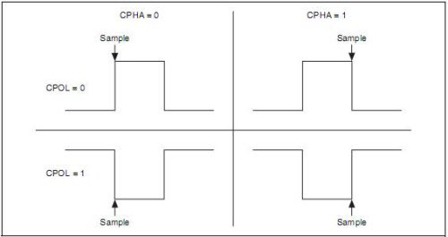
Parameters called clock polarity (CPOL) and clock phase (CPHA) determine the edges of the clock signal on which the data are driven. These two parameters have two possible states, which allows for four possible combinations, all of which
are incompatible with one another. A master/slave pair must use the same parameter pair values to communicate. If multiple slaves are used that are fixed in different configurations, the master will have to re-configure itself each time it needs to communicate with a different slave
- CPOL controls whether the clock start out high or low when the transmission begins. If CPOL = 0 the clock starts low and a rising edge is the first edge of the clock after the SS line is set. If CPOL = 1 the clock starts high and a falling edge is the first edge for the transmission
- CPHA controls whether the devices take a data sample from the MOSI and MISO line on the first edge or second edge of the clock. CPHA = 0 means first edge and CPHA = 1 means second edge. Remember the first edge being rising or falling depends on the CPOL parameter.
Figure 4: This figure shows the four combinations of CPOL and CPHA and how they affect the polarity of the SCLK line and the edge on which the devices sample the MISO and MOSI lines.
SPI Timing Considerations
All hardware devices that can communicate using SPI have timing boundaries which give tolerances for the speed, setup, and hold times of each signal. A typical device has the important signal specified like the example in the images below.
Figure 5: This figure show the different signal timing characteristic that usually have tolerances specified on a data sheet.
Figure 6: This table is a example of hardware specifications for Min and Max times for the clock speed, setup, and hold time.
The RMC Digital IO Capabilities white paper provides a detailed example of timing analysis for synchronous interfaces such as SPI.
Strengths and Weaknesses of SPI
Strengths
- Widespread support and IP available
- Full duplex communication
- Higher throughput than I²C or SMBus
- Complete protocol flexibility for the bits transferred (i.e. Not limited to 8-bit words)
- Simple Protocol to implement and understand
- Typically, no external circuitry required (unlike I²C which requires pull-up resistors)
- System clocked by a master meaning that precision oscillators and PLL not needed
- Addressing not needed (decreases complexity and helps throughput by not sending an address for each communication)
- Transceivers are not needed
- Serial protocol use fewer physical connections than parallel interfaces
- Mostly shared lines for multiple devices (except the separate SS lines for each device)
Weaknesses
- No standards body governs SPI as an official protocol, leading to vendor-specific implementation inconsistencies
- The more devices you have the more pins and connections necessary
- No hardware flow control
- No hardware slave acknowledgment (the master could be "talking" to nothing and not know it)
- Does not support a multi-master architecture
- Only handles relatively short distances (typically intended for on-PCB communication)
Browse, Download and Share SPI Device Drivers and FPGA IP
You have a number of options from National Instruments for communicating using SPI. VI Package Manager hosts IP libraries for NI hardware programmable with LabVIEW FPGA. Software drivers have also been created for Digital I/O and Multifunction Data Acquisition devices, and the USB-845X SPI devices to communicate SPI directly from a PC or Real-Time system. The table below links to detailed information regarding SPI with appropriate hardware and software tools.
| Software Reference | NI Hardware | Description |
| LabVIEW FPGA SPI IP - VIPM | NI Hardware Programmable with LabVIEW FPGA | Download LabVIEW FPGA SPI IP from the VI Package Manager. This FPGA IP works for any hardware enabled by the LabVIEW RIO architecture, including R Series, CompactRIO, Single-Board RIO, and FlexRIO. |
| SPI for Hardware-timed Digital I/O Boards | Digital I/O Hardware Products | Tutorial and SPI driver code for hardware-timed Digital I/O boards like the 6547, 6548, 6551, 6552, and 6556 devices to communicate using the SPI protocol
|
| SPI for USB-8451 SPI/I2C USB Device | LabVIEW example and a tutorial for using the USB-8451 or USB-8452 to communicate with SPI devices |


