Onboard Signal Processing (OSP) on National Instruments Signal Generators
Contents
- Overview
- Benefits of OSP
- Onboard Signal Processing Functions
- FIR Filter Types
- Conclusions
- References
Overview
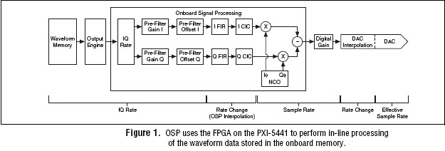
Modern communications systems rely on creative, intensive digital signal processing to maximize channel efficiency, minimize power consumption, and improve link quality and throughput. Traditionally the signal processing was done by a DSP or ASIC, but with the advent of high-gate-density field-programmable gate arrays (FPGAs), the flexibility of a DSP and the parallel processing power of ASICs can be realized in a single device. The National Instruments PXI-5441 arbitrary waveform generator and NI PXI-5671 RF vector signal generator make use of FPGA technology to efficiently process or create communications waveform data on the modules themselves, as opposed to using the general-purpose processor of the host computer. The onboard signal processing (OSP) of the PXI-5441 and PXI-5671 (Figure 1) significantly extends waveform playback time and reduces the time required to compute and download waveform data by computing the waveform data using an FPGA. The OSP block delivers several signal processing functions used to modify the data stored in waveform memory during generation. OSP functions include finite-impulse response (FIR) and cascaded-integrator comb (CIC) interpolation filters, digital prefilter gain and offset control, a numerically controlled oscillator (NCO), and IQ mixing for quadrature digital upconversion. Using these processing functions, OSP delivers four main functional modes
• Quadrature digital upconversion with signal impairments
• Baseband signal interpolation
• Direct double sideband amplitude modulation
• Function generation
Benefits of OSP
The OSP delivers four main benefits
• Reduced computational and download times of waveforms to onboard waveform memory
• Longer waveform playtimes
• On-the-fly signal adjustments such as signal impairments and frequency changes
• Linking and looping of baseband waveforms
The OSP effectively transfers the creation of waveforms from the host PC to the hardware, thus reducing the computational and download times significantly. The following scenario depicts a typical use case. The computation and download of a waveform representing a 65,000 sample 3.84 MS/s QPSK signal generated at the maximum sample rate of 100 MS/s takes more than 85 s using the host PC processor (PXI-8187 controller with 2.5 GHz Pentium 4 running Windows XP). The computation and download time of the same waveform using OSP takes under 10 s; an >8.5X improvement. Additionally the waveform memory requirements are reduced significantly as well. The host PC method takes up to 3.15 MB of onboard memory whilst the OSP method takes up to 0.5 MB; a 6.3X improvement. This is because the host PC method creates the root raised cosine pulse shaped waveforms from I/Q chip data and resamples it to a 100 MS/s sampling rate, thus taking up considerable waveform memory. The OSP creates the waveforms on the fly from I/Q chip data stored on the onboard memory. The pulse shaping, interpolation, and upconversion of the data at baseband to an IF frequency is done in line - the data is fed to the OSP at the symbol/chip rate and the OSP feeds the waveforms at 100 MS/s to the DAC.

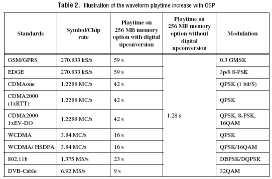
The following table illustrates some of the common communications applications the waveform playtimes possible on the PXI-5441 and PXI-5671, allowing for large PN sequence signal generation for enhanced bit-error-rate test (BERT) of receivers.
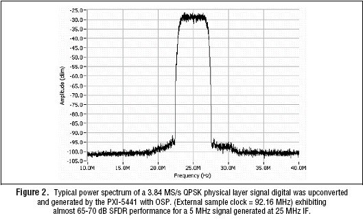
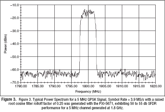
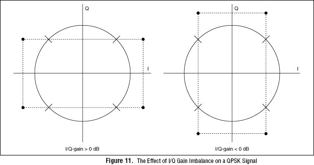
And the OSP delivers on-the-fly signal impairments, which allows things such as I/Q gain, offset, and quadrature skew discussed in detail later in this paper.
Quadrature Digital Upconversion with Impairments
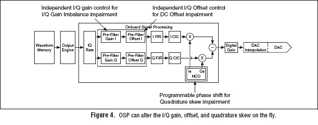
In quadrature upconversion, I and Q complex waveform data is stored in waveform memory and is passed to the OSP block. OSP then shapes and interpolates the data using the FIR filters, interpolates it up to a high sample rate using the CIC filters, and then up-converts the data to a programmable carrier frequency up to 43 MHz. You can choose to suppress the lower or upper modulation sideband by adjusting the NCO in-phase and quadrature output phase settings.
For modeling channel effects and testing the robustness of a receiver, the OSP can add several impairments to the signal on the fly (during waveform generation). IQ gain imbalance and DC offset impairments are implemented by adjusting the one-filter gain and offset settings, while quadrature skew and frequency error can be introduced by adjusting the I or Q carrier phase and frequency.
Baseband Interpolation for I/Q Signal Generation
Useful for generating baseband signals, such as I and Q signals, you can use the PXI-5441 OSP block to interpolate low-data-rate waveforms to a much higher sampling rate, thereby improving the output frequency spectrum by relocating zero-order sample-and-hold reconstruction images to higher frequencies. With the images at higher frequencies, the seventh-order lowpass analog filter in the PXI-5441 can greatly suppress them without disturbing the amplitude or phase of the signal. For example, a waveform created at 3 MS/s sampling rate can be interpolated to 96 MS/s by using 4X FIR interpolation and 8X CIC interpolation. The upsampled signal is then passed to the DAC which can also interpolate by 2, 4, or 8X resulting in an effective sampling rate of 384 MS/s (4X DAC interpolation). The resulting sampling rate of 384 MS/s places the sampling images well above the lowpass analog filter cutoff frequency, thus effectively attenuating the images. Because the original waveform was sampled at only 3 MS/s, rather than 96 MS/s, a 1:32 compression ratio is achieved, resulting in dramatically faster waveform computation and download times. The resulting compression can be used to efficiently store data in the PXI-5441 onboard memory so that you can achieve much longer playback time without streaming from arrays of high-speed disk drives. Long playback times are essential for improving the statistical significance of many communications measurements and displays such as bit error rate, CCDF, trellis plots, and constellation plots.

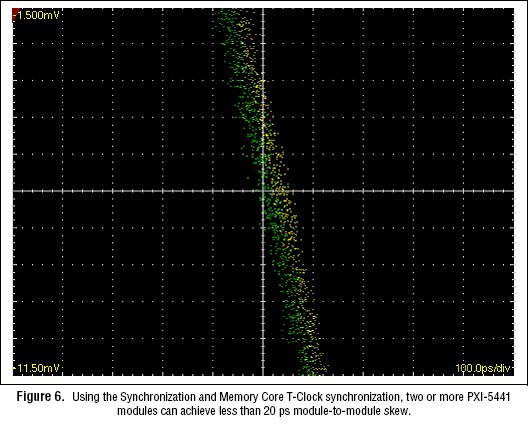
Using T-Clock synchronization technology, multiple PXI-5441 modules can be synchronized for applications requiring a greater number of channels, such as I/Q signal generator or multiple IF generation for MIMO systems. Because it is built into the SMC, T-Clock can synchronize the PXI-5441 with SMC-based high-speed digitizers and digital waveform generator/analyzers for tight correlation of analog and digital stimulus and response. Using onboard calibration measurements and compensation, T-Clock can automatically synchronize any combination of SMC-based modules with less than 500 ps module-to-module skew. Greatly improved from traditional synchronization methods, the skew between modules does not increase as the number of modules increases. To achieve even better performance, a high-bandwidth oscilloscope such as the Tektronix CSA8000 Communications Signal Analyzer can be used to precisely measure the module-to-module skew. Using the oscilloscope measurement for calibration information, T-Clock can achieve <20 ps module-to-module skew (Figure 6).
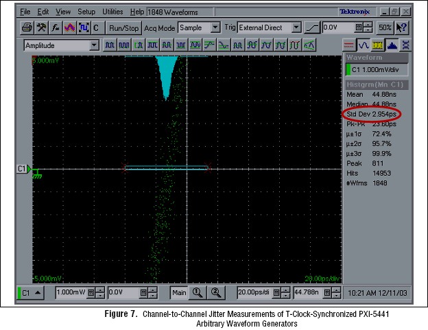
Channel-to-channel jitter is also an important consideration for I/Q signal generation. Significant jitter leads to unwanted quadrature skew and gain imbalance. The total system jitter between two PXI-5441 outputs is less then <20 psrms (Figure 7) thus allowing for wideband I/Q signal generation.
Creating I/Q Data for Use with OSP
A number of additional tools exist to create I and Q waveform sample data. Commonly, data resulting from simulations using a math package such as MATRIXx X-Math are stored to disk. National Instruments LabVIEW and LabWindows/CVI can read a variety of data file types and convert them to either I16s or complex double-precision floating-point numbers - two formats that the NI-FGEN driver directly accepts. By first normalizing the waveform data to ±1 V and extracting the gain multiplier, the AWG can use the full 16-bits of the DAC and amplify or attenuate the output signal using the front-end analog electronics to ensure the best output signal quality.
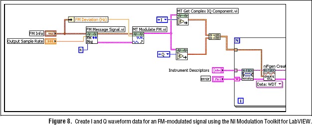
LabVIEW can also directly generate I/Q data using the NI Modulation Toolkit. The Modulation Toolkit provides LabVIEW VIs for modulating and demodulating both analog and digital schemes such as AM, FM, PM, QPSK, and QAM. Figure 8 shows how to use the toolkit to create I and Q data for a frequency-modulated (FM) signal. With the first VI, you generate the FM message signal by selecting from standard waveforms such as sine, square, or triangle, and specifying the carrier frequency and frequency deviation. The next VI performs the modulation and returns the complex envelope of the FM signal. Lastly, two VIs extract I and Q data from the complex envelope signal and download it to two T-Clk synchronized arbs. The toolkit can also modulate a user-defined message signal and extract the modulated signal magnitude and phase (polar form) components to test a polar-based digital modulator. The programming for creating waveforms with different modulation schemes (such as QAM and QPSK) follows a similar structure.
To model channel effects, the Modulation Toolkit offers Rayleigh and Rician fading profiles; or you can create your own custom-defined fading profile based on the simulation tool output.
Double-Sideband Amplitude Modulation (AM)
By using only the in-phase (I) path of the OSP block, one can generate an AM signal by directly downloading the message signal into onboard memory. The message signal scales the amplitude of the programmable frequency output of the NCO.

Single-Tone and Function Generation
Using the OSP NCO, the PXI-5441 can generate sine, square, triangle, ramp and other standard and user-defined waveforms similar to function generators (The PXI-5671employs the NCO to generate RF tones). The benefit of using the OSP for function generation is elimination of waveform creation and downloads to the onboard memory for function generation and phase-continuous frequency changes. For example a tone with <50 Hz resolution may require many cycles of a sine waveform to be downloaded for generation at 100 MS/s, consuming valuable host PC processor and onboard memory resources. With the NCO, no waveforms are downloaded to arbitrary waveform memory. (For further information on NCO functionality please refer to [6].)
The frequency of the output waveform may be adjusted during generation with 355 nHz resolution for generating phase continuous frequency sweeps and hops. The phase is also adjustable relative to other synchronized instruments, the PXI 10 MHz reference clock or an externally supplied reference clock.

Onboard Signal Processing Functions
Independent I and Q Prefilter Gain and Offset
Because of slight component mismatches, I and Q signal paths of a physical communications system where I and Q are handled in the analog domain invariably have some mismatch in skew, gain, and DC offset. To model this effect, OSP has independently controlled prefilter gain and DC offset parameters. This capability is particularly useful during the prototyping and verification stages of product development to evaluate receiver sensitivity/immunity to impairments. These parameters can be set before or during signal generation.
To see the effects of I/Q gain imbalance on a digitally modulated signal, consider a QPSK signal. The ideal symbol coordinates of a QPSK signal would lie on the unit circle when plotted as a constellation diagram in the I/Q domain. When I/Q gain imbalance is applied, the symbol constellation distorts vertically or horizontally (Figure 11).
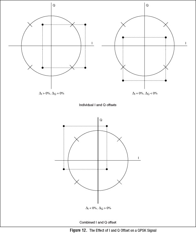
DC offset is a complex signal impairment that shifts the locus of the ideal symbol coordinates off center in the I/Q plane. A DC offset can be added to the I component, the Q component, or both. The DC offset can be either positive or negative, with the sign indicating direction of the shift (Figure 12).
Numerically Controlled Oscillator (NCO)
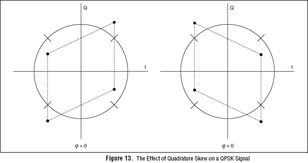
The NCO is a digital circuit that creates two discrete-time, discrete-valued representations of sine waves of the same frequency (the carrier frequency) with two independent phases. The OSP NCO produces sine and cosine waveform data for quadrature digital upconversion and features 355 nHz frequency resolution and 0.0055º phase resolution. To add quadrature skew, also called quadrature error, to a quadrature-modulated signal, the phase of the sine and cosine outputs of the NCO can be independently adjusted. Quadrature skew describes a complex signal impairment such that the I and Q components are not perfectly orthogonal and appears as a “twisting” in the IQ domain constellation diagram (Figure 13).
Digital Interpolation
Interpolation of waveforms sampled at low data rates to high sample rates for digital-to-analog conversion is achieved with a FIR filter and a CIC filter. Multistage filter structures are more efficient than single-stage filters. A multistage filter gradually increases the sampling rate by passing the signal through two or more resampling stages. Each stage has a lower interpolation factor, which enables the required transition bandwidth of each stage to be substantially relaxed. Because each stage contains fewer operations, the filter order of each stage is also reduced which reduces the complexity of the overall filter. The FIR filter interpolates the waveform up to 8X and the CIC filter can further interpolate up to 256X delivering a total interpolation factor of 2048X.
The FIR filter plays three important roles – it interpolates and pulse shapes the waveform to address intersymbol interference (ISI) and compensates for the CIC filter frequency response. CIC filters are used to achieve the large sample rate changes. They are typically used in applications that have a high sample rate that is redundant; the system sample rate is much larger than the bandwidth occupied by the signal. The following two section discusses the FIR and CIC filters in more detail.
Finite-Impulse Response (FIR) Filter
The OSP FIR filters are used to pulse shape I and Q data for more efficient frequency spectrum usage and compensate for the CIC filter response. The FIR filter structure, as opposed to the IIR filter structure, is frequently used in communications systems because of several of its properties:
• Exactly linear phase response is possible with symmetric coefficients.
• Guaranteed stability because feedback is not used.
• Easily implemented in FPGAs.
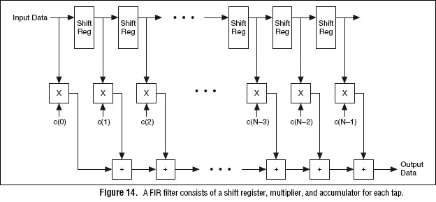
The structure of the FIR filter is a long shift register. Each tap in the shift register is multiplied by an associated coefficient (c(x) in Figure 14). The results for all of the taps are then summed to create the final output of the filter. The OSP FIR filter has 95 taps with 17-bit filter coefficients for precise control of the filter response.
In communications applications where phase is often used to encode data, filter phase linearity is crucial and is the main driver behind using FIR filters. To determine FIR coefficients for linear phase, the coefficients must be symmetric. Thus, the first and last taps have the same coefficient, the second and second-to-last taps have the same coefficient, and so on. The FIR filters in the OSP block are symmetric. Because the FIR filter in the OSP has an odd number of taps, the center tap does not have a matching tap.
The final purpose of the FIR filter is to interpolate the waveform data by 2, 4, or 8X. This process involves two steps:
• Inserting samples with a value of zero in between data samples (upsampling).
• Passing the resulting waveform through the FIR filter.
By interpolating, the sample rate of the data is increased, which results in better spectral performance once the samples are converted by the DAC into an analog signal.
Pulse Shaping
The need for pulse shaping can be readily understood by examining a straightforward implementation of a digital transmitter. This transmitter would switch on an energy source of a fixed duration to transmit a “1” and would switch the energy source off to transmit a “0”, resulting in an irregular pulse train when viewed in the time domain. The power spectrum of such a signal resembles the sinc function and the signal theoretically occupies infinite bandwidth (Figure 15). This is a direct result of the sharp pulse edges in the time-domain signal.

To increase transmission speed without decreasing accuracy or increasing bandwidth, rectangular pulses can be shaped into more suitable signals by using a filter. The raised cosine pulse and root raised cosine pulses are two such pulse shapes that improve spectral efficiency (Figure 15). As with all physical systems, this saving comes at the expense of another design parameter – complexity. As opposed to the elegant simplicity of simply switching on and off an energy source to create a rectangular pulse signal, transmitters and receivers for pulse-shaped signals are much more complex and susceptible to jitter. Careful design must be used to maintain adequate link margin when more complex pulse shaping methods are used to improve spectral efficiency.
FIR Filter Types
OSP includes FIR filter coefficients for flat, raised cosine, root-raised cosine, and Gaussian responses. It is also possible to load custom filter coefficients.
Flat
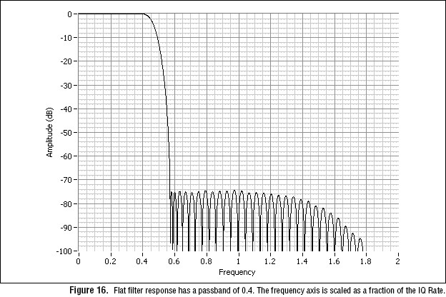
When using OSP to interpolate baseband data to higher sample rates, the flat response is often the proper filter response type. The flat response is designed to give a flat response until the specified passband value. For instance, with the interpolation rate set to 4X, the filter passband ripple is 0 to –0.08 dB with 74 dB out of band suppression. The passband value is a fraction of the IQ rate of the data coming into the FIR filter and can be up to 0.43 × (IQ Rate).
Raised Cosine
The raised cosine filter type is frequently used in digital communications to increase the efficiency of bandwidth usage by confining the signal power within the specified band. The ideal frequency response of a raised cosine filter consists of unity gain at low frequencies, a raised cosine shape in the middle, and zero gain at high frequencies. The following equation describes mathematically the magnitude response of a raised cosine filter.
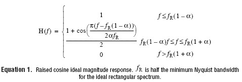
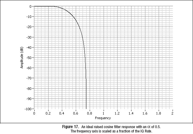
The sole parameter in specifying the characteristics of raised cosine filter is (a ), also called the “roll-off factor.” The passband of the raised cosine filter stops at 0.5 × (1 – a ) of the IQ Rate. The stop-band of the raised cosine filter begins at 0.5 × (1 + a ) of the IQ Rate.
Root-Raised Cosine
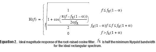
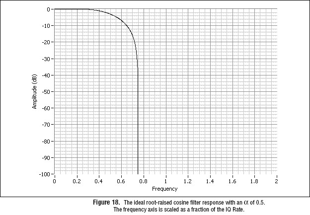
To split the overall raised cosine filtering evenly between the transmitter filter and receiver filter, use the root-raised cosine filter. This configuration maximizes the signal-to-noise ratio (SNR) while minimizing ISI. This filter is used in W-CDMA and DVB (digital video broadcast) standards as well as many others. As with the raised cosine filter, the magnitude response characteristics of a root-raised cosine filter are controlled by á. For á = 0, the filter response would be identical to the ideal Nyquist “brick-wall” filter. Such a filter is not possible to construct: OSP supports from 0.1 to 0.9. The following equations illustrates the magnitude response of the root raised cosine filter.
Custom
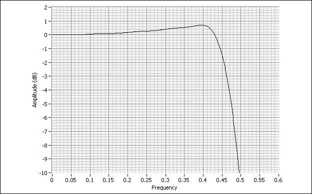
OSP also accepts user-defined FIR filter coefficients. This capability is especially useful for researching and prototyping new transmitter designs. OSP has 95 symmetrical coefficients defined for the FIR filter. To design a custom OSP FIR filter, the coefficients must be correctly scaled and compensate for CIC filter rolloff.
Cascaded-Integrator Comb (CIC) Filter
A CIC filter is designed to efficiently interpolate waveform data by large factors. Interpolation, or upsampling, is the process of increasing the sampling rate of a signal to a higher integrally related sampling rate. The signal spectrum of the output signal is the same as the input signal spectrum, except that a high frequency region with zero power density is added. Most of the interpolation in OSP is done in the CIC filter, which has an interpolation range of 6X to 256X. The CIC filter is a series of combs (differentiators) followed by a zero stuffer, followed by a series of integrators.
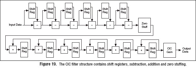
The transfer function demonstrates that a CIC filter is equivalent to N-stage cascaded FIR filters. Because all the coefficients of the FIR filters are unity, and therefore symmetric, a CIC has a linear phase response and constant group delay exactly like linear phase FIR filters. The frequency response (in dB) of the CIC follows the following formula:
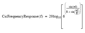
where
R = CIC Interpolation Rate
f = Frequency (fraction of CIC input sample rate)
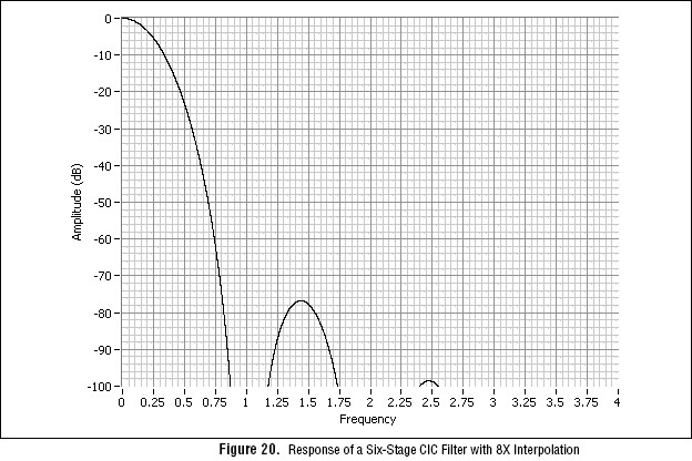
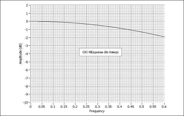
In Figure 20, notice that the frequency response has a significant amount of roll-off in the passband. You must compensate for CIC roll-off in the FIR stage to obtain an overall flat response.
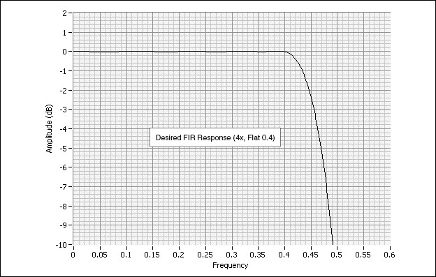
For example, if you want a net interpolation of 32X, the FIR filter interpolation factor is set to 4X and the CIC interpolation factor is set to 8X.
The following diagram shows the desired response from the FIR with 4X interpolation.
However the CIC has the following response:
The CIC compensated FIR response is designed as follows:
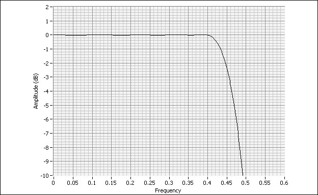
Thus, the final response after the FIR (with CIC compensation) and CIC filters is the desired frequency response.
Conclusions
The NI PXI-5441 arbitrary waveform generator and NI PXI-5671 RF vector signal generator make use of FPGA technology to efficiently process or create communications waveform data on the module itself as opposed to using the general-purpose processor of the host computer. The benefits are increased playtimes, higher throughput for automated test, and reduced computational demands on the Host processor.
References
1. Duraiappah, Lokesh, National Instruments Synchronization and Memory Core- A Modern Architecture for Mixed Signal Test White Paper (National Instruments, Austin TX), 2003
2. Duraiappah, Lokesh, National Instruments T-Clock Technology for Timing and Synchronization of Modular Instruments White Paper (National Instruments, Austin TX), 2004
3. Anderson, Brian, Benefits of Using SMC-Based Arbitrary Waveform Generators for IQ Signal Generation White Paper (National Instruments, Austin, TX), 2004
4. Gentile, Ken., “The care and feeding of digital, pulse-shaping filters” RF Design Magazine, April 2002.
5. Communication Systems: Analysis and Design by Harold P.E. Stern and Samy A. Mahmoud, Prentice Hall PTR
6. A Technical Tutorial on Direct Digital Synthesis, Analog Devices Inc. 1999
7. Donadio, Matthew, CIC Filter Introduction(http://www.dspguru.com/info/tutor/cic.htm), 2000
8. National Instruments Digital Filter Design Toolkit User Manual
9. National Instruments Modulation Toolkit Online Documentation