Understanding Direct Digital Synthesis (DDS)
Overview
Learn the fundamentals and theory behind direct digital synthesis and how it applies to function generators and arbitrary function generators.
Contents
Introduction
The Generating a Signal white paper explores the beginnings of how signal generators, such as function generators and arbitrary function generators (AFGs), output a wanted analog signal and how some signal generators use direct digital synthesis (DDS) technology to output signals at precise frequencies. This article discusses the components and technology that give signal sources the ability to achieve sub-Hertz accuracy in signal generation.
Theory of Operation
Signal generators that use DDS generate signals at precise frequencies through a unique memory access and clocking mechanism, which differs from the traditional method of outputting each sample in the order of which the waveform is stored. Arbitrary waveform generators (AWGs) use the traditional signal generation method. AWGs can produce complex user-defined waveforms, but are limited in the frequency precision at which the waveform is generated. This is because of the constraints that the waveform must produce point by point from the AWG’s memory and the sample clock controlling the time between each point generated has a finite number of frequencies.
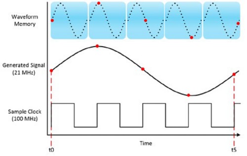
Function generators and AFGs that use DDS store a large amount of points for a single cycle of a periodic waveform in memory. DDS technology gives the function generator or AFG the ability to choose which sample to output from memory. Because the function generator or AFG is not restricted on choosing the next sample in the waveform, it can produce signals at precise frequencies. Figure 1 graphically represents how a function generator or AFG can produce a 21 MHz sine wave, which is not an integer division of the 100 MHz sample clock. The 100 MHz sample clock still drives the update rate of the DAC output; therefore, the faster the sample clock, the more accurate the shape of the created signal.
Figure 1: In DDS-capable hardware, the samples are not necessarily chosen in the order they are stored in memory. This allows the 100 MHz sample clock to accurately create the 21 MHz sine wave
In the specific case above, the AFG uses the 100 MHz sample clock to drive the DAC but the frequency of the signal generated is created by the method of which the samples are chosen from the waveform memory location. The next sections discuss the components that implement the controlling logic behind the sample choice.
Functional Overview
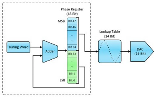
DDS implementation requires three main hardware building blocks: a (a) sample clock, (b) phase accumulator, and (c) lookup table, which is an implementation of a programmable read-only memory. Figure 2 shows the higher level flow from hardware block to hardware block.

Figure 2: Hardware Block Diagram for the DDS Architecture
a. Sample Clock
The sample, or reference, clock is used to create the frequency tuning word, update the phase accumulator value, and drive the digital-to-analog conversion. The sample clock determines when a sample is output by the DAC, but it does not directly determine the frequency of the output signal.
b. Phase Accumulator
The phase accumulator is a collection of components that allows a function generator or AFG to output at precise frequencies. To create the signal at a precise frequency, the phase accumulator uses three general components. First, the phase accumulator uses the tuning word to specify the frequency of the signal. The tuning word is a 24- to 48-bit digital word that specifies how many samples to jump in the waveform memory. The second component, the adder, takes the tuning word and sums it to the phase register remainder. This new digital value is output to the phase register. The final component of the phase accumulator, the phase register, takes the new digital word and uses it to specify the memory address of the next sample point to be output in the lookup table. The phase register takes the remaining most significant bits not used in the lookup table memory address and provides them back to the adder to ensure frequency precision over time.
c. Lookup Table
The output of the phase register only looks like a digital ramp as the memory address increases over time, which is changing at the rate specified by the tuning word. Therefore, to output the wanted waveform, the output of the phase register points to the needed waveform sample address in the lookup table. The lookup table then provides the digital word at the provided memory address, which is the digital word of the correct amplitude and phase for the DAC to produce.
Frequency agility, or the ability to change the waveform’s frequency very rapidly and phase continuously, is one of the main benefits to the DDS architecture. An AFG using DDS can change the waveform’s frequency very rapidly because only the tuning word needs to be changed in order to change the waveform’s frequency.
Common Applications
As discussed above, DDS technology provides two main benefits. One major benefit of DDS technology is the frequency accuracy of the generated signal. This capability opens the door to extremely accurate component testing because you can rely on the frequency accuracy of the function generator or AFG-created signal.
The capability to change the generated signal’s frequency extremely rapidly and phase continuously is the second main benefit of DDS technology. This allows for more efficient component testing over specific ranges because you can implement the frequency change quickly and also stress test devices by pushing the limits on what signal they are providing to the device under test.
A specific example where AFGs with DDS technology are extremely valuable is accurate filter characterization. The characterization of the filter is only accurate if the signal provided to the filter is generated precisely by the AFG and if the filtered signal is accurately measured by an oscilloscope. Figure 3 represents a typical test setup for filter characterization.

Figure 3: Filter Characterization Application Block Diagram With a DDS-Capable Function Generator, a Lowpass Filter, and an Oscilloscope
Summary
- Signal generators without DDS technology produce waveforms by outputting the stored waveform point by point at the frequency of the sample clock.
- Signal generators with DDS technology can produce periodic waveforms at many frequencies with extreme frequency accuracy. This is because of the unique memory access and clocking mechanism.
- DDS technology is implemented with three higher level hardware blocks: the sample clock, the phase accumulator, and the lookup table.
- The sample clock creates the frequency tuning word, updates the phase accumulator value, and drives the DAC output rate.
- The phase accumulator takes the frequency tuning word as input and provides the digital memory address of the next sample to be output in the lookup table.
- The lookup table stores the periodic waveforms as digital samples. The lookup table takes the memory address from the phase accumulator and provides the digital waveform sample at that memory address to the DAC.
- Signal generators with DDS technology should be used for applications that require precise frequency generation or frequency agility.
- Applications that require extremely large, complex, and user-defined waveforms may be best served by arbitrary waveform generators instead of arbitrary function generators with DDS technology.
