The NI PXI-4110 Programmable Power Supply Architecture - Speed, Power, and Precision in 3U PXI
Overview
As programmable power supplies evolved into mainstream components of automated test systems in the last 20 to 30 years, the design of each device has been somewhat limited to one of two basic architectures, switching and linear regulation. As in any product development, tradeoffs are required when choosing each design; both switching and linear regulation offer numerous opportunities to trade off performance. The task of creating a power supply the size of 3U PXI, however, forces an innovative approach. This paper discusses the novel design characteristics of the NI PXI-4110 triple-output programmable DC power supply and the unique combination of switching, linear regulation, and software-defined hardware that make the design possible in a small package.
Contents
- Linear versus Switching Regulation
- Designing into a 3U PXI Module
- Switching Regulation with Linear Output
- 20 mA Current Range for Precision Source Applications
- Supplying Input Power to the PXI-4110
- Protecting the PXI-4110 Inputs and Outputs
- Maximized Programming Speed
- Conclusion
Linear versus Switching Regulation
The earliest programmable power supply designs all focused on linear regulation to provide a steady output voltage. They involved power transistors operating in the linear (class A) mode with feedback setting the output characteristics. Based on a fairly simple design concept, linear power supplies have the advantage of very precise regulation, low ripple and noise, and excellent response to line and load changes. However, their drawbacks make them largely undesirable for a PXI-based power supply design - large physical size, low efficiency (ranging from 5 to 60 percent), and consequently, large power dissipation. While the PXI specification allows about 20 W of cooling per slot, this would not be enough to provide the traditional power required for ATE systems.
A more recently accepted method of delivering accurate power in test systems has come from switching regulation. Switching regulation involves transistors rapidly commutating on and off with their duty cycle determining the output voltage. Consequently, the timing regulation on the transistors will determine the precision of the output voltage. This method offers the advantage of much greater efficiency than their linear counterparts, often in the range of 65 to 90+ percent, and therefore yields much cooler designs. The typical weight of each component is also much lower, keeping the physical package in check. However, optimum transient response tends to be more difficult to obtain, and the electromagnetic interference from the switching components must be considered. Finally, with the above factors combined, it is still difficult to compete with the low output noise and speed possible with linear designs.
Designing into a 3U PXI Module
So, how does one solve the problem of designing a highly efficient power supply in an extremely confined space while delivering the high performance that customers expect? The space constraints of a single-slot PXI module for a precision power supply do not allow much room for large, cumbersome heat sinks and lossy big-iron transformers. NI engineers took the approach of combining the traditional linear output approach with a novel, FPGA-controlled preregulator circuit to meet these design constraints. Let's look at this in more detail.
Modern switching power supply technology has improved dramatically over the 30 lb power supplies of yesterday. Technically, small size in power supplies is dictated largely by switching speed. As a general rule, the higher the switching speed, the smaller the magnetic components. In the mid to late-1980s researchers at the Massachusetts Institute of Technology and elsewhere were experimenting with the concept of 1 MHz switching converters, amplifiers. and regulators. Within the last five years, this technology has exceeded even those expectations. However, progress is minimized if the switching elements are so lossy that any improvement in component size is negated by the need to heat sink the switching elements due to inefficiencies. Here again, technologies have improved dramatically over even the last 10 years. Combined with new power supply controller integrated circuits, the stage is set to synthesize efficient, high power, and even quiet power supplies that do the job of their old, traditional big-iron counterparts.
So far, however, this technological evolution gets us only raw quasi-regulated power. There are still design challenges, including the ability to program to 0 V, sense currents from microamps to amps, provide rapid response to load and programmed inputs, and so on. The best way to solve these problems (and provide exceptional noise performance) is with traditional linear circuitry. So the best overall solution is a marriage of both linear and switching technologies.
As an aside, off-the-shelf Class D amplifiers are also an option for high-performance power supply designs. Unfortunately NI engineers determined that while these are innovative devices for audio applications such as efficiently driving speakers, they have limitations where precision DC outputs are required. In our judgment, these limitations outweigh the potential gains that they might offer.
Switching Regulation with Linear Output
The NI PXI-4110 triple-output programmable DC power supply combines traditional linear and switching power technologies by configuring the switcher as a tracking regulator, essentially creating a rail with variable headroom above the programmed output. The end result is a module with two isolated channels, one from 0 to +20 V and the other from 0 to -20 V, and a single nonisolated channel from 0 to 6 V, all capable of putting out up to 1 A per channel. These basic power output specs are complemented by excellent resolution and low noise for the PXI-4110 as a voltage or current source.
The linear output control of the PXI-4110 is depicted in Figure 1. The core technology in the linear stage is the Linear Technologies LT1970 power op amp with adjustable precision current limit. The LT1970 has several advantages for a PXI power supply implementation, not the least of which being its small size and "on the fly" current limit, which is specifically helpful for ATE applications. Traditionally, this was referred to as a "VI control block" because it allowed the output to be constant-voltage or constant-current controlled, depending on the input settings and output load; it was implemented with discrete op amps, diodes and resistors. This VI control block forms the heart and soul of traditional source/measure units (SMUs). Thus, using the LT1970 VI control block helps give the PXI-4110 SMU-like behavior.
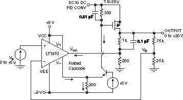
Figure 1: The Linear Technology LT1970 is the heart of the PXI-4110 voltage/current control block.
Because more output voltage and current were required than the LT1970 could provide, analog "translator" circuitry was designed to handle the output range. It was necessary to scale both the output control and the measurement in this fashion. Figure 2 shows the basic blocks that represent this dual-direction translation. In the design of this translation, it was important to keep in mind several critical details:
- It is necessary to bring the output all the way to 0 V
- We must be able to measure both voltages and currents all the way to 0 V with submicroampere leakages
- We must sink enough current from any output load or capacitance to maintain good response time even near 0 V
- We must be able to tolerate input overvoltage conditions
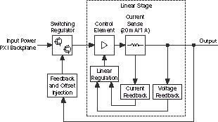
Figure 2: The linear regulation stage is designed to source/measure very low voltages and currents.
The LT1970 acts as an op amp to drive the discrete output devices providing the translation to the required output voltages. Using a discrete MOSFET output element for each channel, output current is boosted to more than 10X the capability of the LT1970 at more than 3X the voltage compliance of the LT1970. Likewise, a high-speed op amp/FET combination is used as a current sense translator to bring the voltage appearing across the current shunts back down to within the LT1970 rails. The result is a fast control loop that delivers excellent transient response and stability over a broad range of loads. This current sense translator is also optimized for dynamic range and noise so that it is possible to sense voltages down to 0 V and currents down to submicroampere levels.
On the nonisolated channel 0, the switching converter is a Linear Technology LT1773 boost-buck converter that provides dynamic regulation of its output. The control output of channel 0 is fed back into the LT1773 through signal conditioning, which results in the LT1773 output "floating" over the channel 0 output by a few tenths of a volt. The result is an extremely power-efficient switching design with all the advantages of a linear regulator.
Directly combining the tracking regulator with the output amplifier described above takes care of the nonisolated channel. With isolated channels 1 and 2, the switching regulator consists of a relatively straightforward high-power DC-DC converter operating at about 200 kHz. The input drive to the converter is synthesized by an FPGA that can vary the duty cycle of the drive signal applied to the switching MOSFETs. The FPGA offers the advantage of intelligent soft-start and ramp-up, which "softens" the transient currents drawn from the PXI backplane, thereby allowing the PXI-4110 to operate within the PXI specification.
Although with the isolated channels there is no direct analog feedback path to the switching regulator control due to the galvanic isolation (see Figure 3), an isolated analog-to-digital converter (ADC) and data path already existed for these channels to provide current and voltage read back. This ADC is monitoring the output voltage and current at all times; so if it can be switched to "look at" the raw input rail supplying the linear output amplifier as well, it is possible to use this signal as isolated feedback. The FPGA can then be used to modulate the duty cycle of the FET drive to the DC-DC converters, effectively providing a digitally controlled, software-in-the-loop PID algorithm to manage the preregulated input to the linear stage. All of this can be done using components that were already needed in the design for other reasons. The result is a cost-efficient, flexible design in a 3U PXI module that can be scaled as additional power supply requirements emerge.
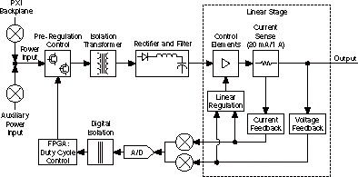
Figure 3: The nonisolated channels on the PXI-4110 make use of analog-to-digital converters to control the switching preregulation elements through the same data path as the current/voltage measurement readback.
There are several advantages to using this software-configurable control loop. First, it is possible to anticipate where the preregulator needs to be before the output amplifier attempts to get there. Figure 4 depicts the importance of implementing this correctly. Second, the response can be tailored to optimize system efficiency. Finally, we can tune the control algorithm to optimize performance depending on whether the input power is coming from the PXI backplane or an external source. It is important that the power being drawn from the PXI backplane be carefully managed to meet the PXI power specifications for the overall product.
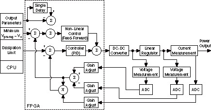
Figure 4: The PID control algorithm implemented in an FPGA on the PXI-4110 analyzes and corrects for all changes in load or input power to ensure the preregulator power output is sufficient for the linear stage.
NI engineers found that regulating the voltage alone was not sufficient. Instead, they determined that the optimal response was obtained by regulating the power being dissipated in the linear regulator. The reason for this is shown in Figure 5. When lightly loaded and run at low duty cycles, DC-DC converters tend to behave more like current sources than voltage sources. When a sudden load is applied to the output of a current source, the output rapidly falls. Thus, more voltage headroom is required to give the PID time to respond. This is accommodated by using power regulation, which automatically adjusts the output voltage headroom to be much larger under light load conditions.
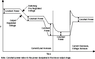
Figure 5: Power is regulated on the PXI-4110 (as opposed to voltage) to compensate for sharp changes in the load. Sufficient headroom is maintained at all times to prevent "crashes" between the preregulator rail and output voltage.
Another example of this flexibility is optimizing power drawn from the input power supply - in this case the PXI backplane. Because the power available from a PXI chassis is limited, it is necessary to provide an auxiliary power source for applications above 9 W. However, many applications exist for power levels less than 9 W, and in those situations, the customer shouldn't be required to supplement the PXI backplane. Using this approach, different PID set points (resident on the FPGA) are used for powering from the PXI backplane versus an auxiliary source. If more power is needed than is available from the PXI backplane, the PID set points are changed to provide a more optimum tradeoff between efficiency and step response.
The design of the PXI-4110 made extensive use of the LabVIEW graphical programming language to simulate the software PID and then translate the code to VHDL to run on the FPGA. This gave the engineers tremendous flexibility in trying out a variety of ideas quickly as various use cases and output load conditions were identified. For example, to guarantee that the preregulated output could respond to an input step change request, the PID was defaulted to a duty cycle that can accommodate the full output load of 1 A for a preset number of clock cycles. Thus, if the combination of requested output state and output load demand full current, the linear output stage will always have enough headroom to accommodate it. The control block diagram and its exceptions would have been difficult to synthesize without the use of LabVIEW as a simulator and "sandbox."
20 mA Current Range for Precision Source Applications
One of the more compelling customer requests to power supply vendors has been current measurement sensitivity in the submicroampere range. Traditionally, power supplies don't measure much below a few mA. To perform these tasks, customers have been forced into SMUs or other measurement products which could cost 2 to 3X the cost of a power supply. With that comes the challenge of integrating additional precision products into the system, possibly with switching and other components, further adding to the cost of the system. NI engineers opted to provide submicroampere level sensitivity to the PXI-4110 to address these needs through the addition of the 20 mA range. This provides output resolution and measurement readback sensitivity 100 to 1000X better than traditional power supplies. This substantially reduces system costs, time to first measurements, and bench space required. Applications for sensitive current measurements include semiconductor device characterization, IV curve tracing, and leakage current tests in battery-operated systems.
Supplying Input Power to the PXI-4110
The market research phase of the PXI-4110 revealed that a good number of applications required only a few watts of output power - a level easily supplied directly from the PXI backplane. Customers were reluctant to supply an external power source for these applications. On the other hand, the power available from a single PXI slot is not sufficient for applications requiring more than about 10 W. So it was decided to make the PXI-4110 capable of both. The NI APS-4100 auxiliary power source was developed as an accessory to the PXI-4110 to accommodate higher-power applications.
Early experiments showed that supporting two power sources for this device would not be a trivial task. For example, if power was being drawn from the external power source and this power was to suddenly disappear, the resulting power surge from the PXI backplane would exceed the PXI specifications (and even trip protective fuses). Appropriate hardware and control software were needed to "lock out" conditions that could cause excessive power to being pulled from or applied to the PXI backplane. Figure 7 illustrates the concept.
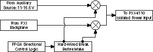
Figure 7: The input power for the PXI-4110 comes from either the PXI backplane or an external 11-15.5 V source.
Protecting the PXI-4110 Inputs and Outputs
In ATE systems and lab settings (including academic environments), the robustness of programmable power supplies is crucial. During ATE system debug, power supply outputs can be inadvertently connected to the wrong places. In lab settings, nodes are often accidentally shorted or connected inappropriately. Thus, the PXI-4110 was designed to accommodate a myriad of overload conditions. The following is a summary of the key protection elements on the PXI-4110:
- Channel Output Protection - Each channel is, of course, current and voltage limited programmatically. In addition, each output is protected against a reverse-polarity voltage application. An output fuse provides additional protection to prevent catastrophic failures as a last line of defense. A spare fuse is available on the board to minimize downtime if it is needed.
- Auxiliary Power Input Protection - An auxiliary power input allows channels 1 and 2 (+20 and -20 V) to supply up to 20 W each. Because the PXI-4110 allows the use of an external power device, appropriate steps must be taken to protect the module.
- Overtemperature Protection - The PXI-4110 is designed conservatively and operates at nominal temperature rise internally due to the intelligent PID control of the output devices. However, if a fault occurs, such as an excessively dirty chassis fan filter, blocked intake, or chassis fan failure, the output channels shut down and a warning is issued. An overtemperature condition requires user software intervention to reset, thus preventing the module from "cooking" at excessive temperatures should such a system fault develop.
Maximized Programming Speed
In automated test systems one of the most important performance attributes of any instrument is speed. For power supplies, the programming and measurement speed as well as the communication bus form the main areas of differentiation for the PXI-4110.
The fact that the PXI-4110 is built around the PXI bus significantly helps optimize programming and measurement speeds. Sending program parameters and retrieving data is greatly facilitated by the 132 MB/s PXI bus speeds. With three channels that each require voltage/current programming and measurement parameters plus status information (compliance limit, warnings, errors, temperature, and so on), the amount of data that needs to be moved in both directions can challenge traditional bus solutions. PXI can move this data in microsecond timeframes compared to several milliseconds or 10s of milliseconds required with traditional instrument bus architectures (GPIB or RS232). Thus, the software and data path overheads are practically negligible for the PXI-4110.
The PXI-4110 measurement architecture is also notable for its speed advantage over traditional measurement approaches. Integrating ADC architectures are traditionally used in power supply measurements. These ADCs have advantages for noise but don't give the user much flexibility to optimize speed, especially "under the hood" in dynamic stimulus-response devices such as precision power supplies or SMUs. With multichannel power supplies, the slower ADC creates significant overhead for acquiring the multiple parameters required to represent the status of the output.
Figure 8 shows the architecture used in the PXI-4110. It is based on similar measurement engines used in National Instruments high-speed data acquisition systems. The ADCs are 200 kS/s, 16-bit high-bandwidth converters - one for the nonisolated channel and another for the two isolated channels. As previously mentioned, the ADCs are used for both measurement read back as well as PID control. The net loop speed of the measurement is in the 3 kS/s range. In other words, every 300 µs, the measurement engine returns six measurements - voltage and current output for each of the three channels (as well as the PID loop data). This is fast enough to watch the settling time of all the channels simultaneously (rise times in the millisecond range) and is faster than required for any stimulus-response step waveforms required by the user.
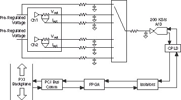
Figure 8: The measurement architecture of the PXI-4110 allows fast readback of voltage/current on each channel before transmitting the data back to the user across the PXI backplane.
Optimum noise performance of the measurement is achieved by averaging multiple measurements. The default is an average of 10, but the user can select and modify that default as needed for the application. The isolated data is rapidly moved over a 10 Mb/s serial data path using high-speed MEMS-based digital isolators.
Conclusion
With the shrinking available space and the high premium placed on performance in the modern automated test system, an innovative power supply design is required to keep pace. The PXI-4110 triple-output, programmable DC power supply uses the best elements of both switching and linear power supply designs to offer a compact, high-resolution source that fits into a single-slot, 3U PXI module. When this product is used in combination with other world-class modular instruments available as PXI modules, it further enhances the user's ability to develop flexible, efficient test systems to meet any challenge in any industry.
Related Links:
NI PXI-4110 Programmable Power Supply
NI Modular Instrumentation