Differences between an NI HSDIO-Based and a Programmable FPGA- Digital Instrument
Overview
Contents
- Why NI HSDIO?
- Why NI FlexRIO?
- Programming a Simple Digital Generation Task in LabVIEW
- Multiple Options for Digital Test
Why NI HSDIO?
Features
Specifications
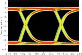
NI HSDIO devices are instrument-class, which means they include detailed specifications that an engineer might expect on comparable high-quality instruments. These devices typically offer features such as eye diagrams, skew specifications, voltage threshold accuracy, and jitter. Figure 1 shows an eye diagram included with the NI PXIe-6548 high-speed digital module.
Figure 1: Eye Diagram of the NI PXIe-6548 at 200 Mbit/s
NI-HSDIO Driver Built-In Features
The NI HSDIO driver provides several built-in features for advanced testing, such as data delay for timing calibration and hardware compare for bit error rate testing. Some of these features are listed below.
 Timing
NI HSDIO instruments provide advanced timing capabilities that offer not only general-purpose digital pattern I/O at finer resolutions but also the capability to characterize semiconductor chips by sweeping timing parameters such as clock frequencies or data deskews. Some of the included features are
- Data delay on data lines, clocks, and trigger/event lines 1
- Source- or system-synchronous clocking
- DDS-based internal clock source with sub-Hz resolution (Gundog and Retriever)
- RTD compensation (Lab and Gundog)
1The NI PXIe-6547 and NI PXIe-6548 feature three banks of data delay, where independent values of deskew can be applied to three banks of physical channels.
 Comparison and Waveform Control
NI HSDIO devices feature built-in comparison features and additional logic states that enable bit error rate testing and compatibility with semiconductor standard patterns and files such as WGL and STIL. With the hardware compare features, engineers can define generation and comparison patterns for stimulus-response tests where the HSDIO device performs a real-time analysis of the response data and reports errors to the user.
These devices also feature a complex scripting engine that engineers can use to loop and link prestored digital patterns with “zero dead time” or no lag between consecutive waveforms. They also can use scripting to perform analysis statements such as IF and WAIT for applications that require the option of choosing between multiple preloaded waveforms or other complex waveform manipulations.
Some of the comparison features are
- Advanced logic states: 1, 0, Z, H, L, X 1
- Onboard hardware compare 2
1 NI 655x and NI 6544/45/47/48 only
2 NI 656x and NI 6547/48 only
 Voltage Levels
NI 655x devices feature enhanced voltage ranges and programmability for tests that require nonstandard logic levels or for tests such as voltage threshold testing and diode testing. These features are ideal for semiconductor characterization or general-purpose digital I/O. These voltage-specific features include
- -2 to 5.5 V
- 10 mV programmability
- Programmable high and low levels
 Synchronization
NI HSDIO devices feature a synchronization and memory core (SMC) daughter card that allows multiple devices to be synchronized within hundreds of picoseconds. The NI-TCLK API allows intuitive and simple synchronization, making channel expansion for analog or digital instruments trivial. Built-in features also include programmable skew between synchronized instruments, offering enhanced channel-to-channel and board-to-board deskew control. The image below shows three simple VIs that engineers can use to synchronize multiple mixed-signal instruments.
 Software
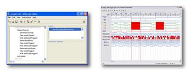
The NI Digital Waveform Editor is a graphical software tool engineers can use to visualize digital signals and easily create, edit, and modify digital waveforms for customized interfacing and test applications.
Figure 2: Tools such as the Script Editor and Digital Waveform Editor make creating and generating waveforms with driver-defined devices easy.
TD-Scan for NI is software engineers can use to import standard semiconductor pattern files such as waveform generation language (WGL) and standard test interface language (STIL). TD-Scan for NI software as well as NI HSDIO hardware features such as hardware compare and extended digital states make the process of taking logic and patterns from standard digital pattern files and generating them on hardware simpler.
Applications
 Characterization
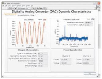
The programmability of voltage and timing parameters on NI HSDIO devices makes them ideal for chip characterization, where sweeping these parameters is required to characterize chips completely. Figure 3 shows the front panel of a LabVIEW VI, where the clock rate is swept from a few megahertz to 200 MHz to characterize the behavior of the digital-to-analog converter (DAC) under these varying clock rates. Similarly, deskew or voltage can also be swept for further chip characterization.
Figure 3: This application characterizes a digital-to-analog converter for dynamic and linear parameters.
 General-Purpose Interfacing
Advanced features such as programmable deskew and voltages make NI HSDIO devices suitable for characterization, but the feature-rich driver also provides an out-of-the-box experience for engineers needing a general-purpose interface to a variety of devices under test (DUTs). The NI HSDIO platform is ideal for general-purpose digital pattern generation, video or image signal generation and acquisition, or logic analysis. NI also provides ready-made solutions for digital audio and video testing called NI Video Measurement Suite (VMS), NI Picture Quality Analysis (PQA), and NI AudioMASTER.
Why NI FlexRIO?
Features
Peer-to-Peer Streaming
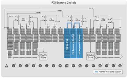
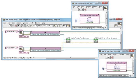
With NI peer-to-peer data streaming technology, engineers can continually transfer data to and from PXI Express NI FlexRIO FPGA modules at rates greater than 800 MB/s with minimal latency. High-performance data switches on NI PXI Express chassis offer high-bandwidth communication, while routing data from one module directly to another (without transferring data through the host controller) minimizes the latency of the transfer.
Peer-to-peer transfers are supported between multiple PXI Express NI FlexRIO FPGA modules and between select NI PXI Express digitizers and PXI Express NI FlexRIO FPGA modules. Figure 3 depicts a peer-to-peer system with an NI PXIe-5122 digitizer and two NI FlexRIO FPGA modules for distributed serial data processing.
Figure 4: Data can be to and from and instrument to an FPGA board for on the fly processing.
With the LabVIEW FPGA Module, engineers can access these peer-to-peer streams through simple first-in-first-out (FIFO) nodes. An easy-to-use API on the host controller sets up a peer-to-peer stream between multiple NI FlexRIO FPGA modules after configuring the peer-to-peer FIFOs.
Figure 5: The NI-P2P driver offers simple, high-level access to the high-performance capabilities of peer-to-peer streaming, while intuitive nodes on the FPGA block diagram simplify data transfer.
IP Integration Node
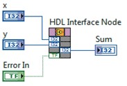
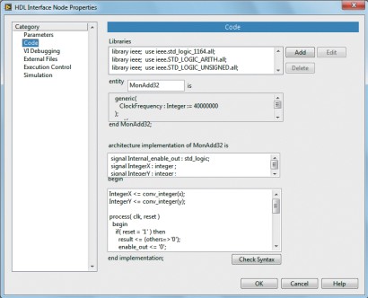
While LabVIEW is an effective tool for FPGA programming, engineers may have existing hardware description language (HDL) intellectual property (IP) that they need to integrate into NI FlexRIO hardware applications. The HDL Interface Node, shown in Figure 6, provides a simple, inline interface to HDL code.
Figure 6: With the IP Integration Node, engineers can import existing IP into NI FlexRIO devices.
Applications
 Digital Protocol Test
Consider the lowest layers of the OSI model – the physical and data link layers. Rather than designing this new bus from scratch, engineers often start with the physical or electrical attributes of an existing bus technology and then customize the higher-level functionality. The physical layer comprises the transmission medium, such as channels, voltages, and connectivity, and the data link layer acts as the functional means of transferring data over the physical layer, including signaling and flow control. Two distinct and incompatible bus architectures may share a physical layer, but they can have very different data link layers.
Decoupling the physical layer from the data link layer is one approach to minimize the amount of custom hardware in communication protocol or bus test systems. FPGAs are ideal for implementing protocols at the data link layer, though their I/O pins may not be optimized for the desired physical layer. This physical layer likely requires additional silicon, perhaps similar to that used in the DUT. With a modular connection between the FPGA and the physical layer over a standard interface, a single FPGA can be programmed to implement a variety of protocols, while various physical layers can be swapped in and out through the standard interface. NI FlexRIO, which provides user-programmable FPGA modules combined with interchangeable I/O adapter modules, is an ideal platform for decoupling the physical and data link layers. Engineers can implement protocols on the FPGA in the abstract, graphical LabVIEW FPGA programming environment, which requires no specialized knowledge of low-level HDLs. I/O adapter modules can be purchased or customized through a module development kit. For example, National Instruments offers the NI 6584 RS422 NI FlexRIO adapter module for RS422 physical layer test. Data link levels such as high-level data link control (HDLC) or synchronous data link control (SDLC) can be implemented on the FPGA, whereas the physical layer is represented by an adapter module such as the NI 6584.
 Custom Tests/Triggering
Many applications require custom algorithms. A very simple example of this is the implementation of a custom serial trigger, which may be challenging to implement on a logic analyzer that has a fixed trigger personality. This logic analyzer might have parallel triggers or an 8-bit serial trigger, but a specific application may require a 16-bit trigger or even a trigger that can dynamically change. Implementing these custom triggers is not easy, if not impossible, on traditional boxed instruments such as logic analyzers or pattern generators. An FPGA in this case becomes an ideal solution because engineers can program the FPGA to their custom requirements, whether it is a 16-bit serial trigger or even a complex video trigger.
Other applications that require such customized algorithms include complex bit error rate testing, where engineers not only require the ability to compare digital data on the fly but also inject errors or implement error correction algorithms such as hamming encoding. Again, in this situation, NI FlexRIO is an ideal solution because engineers can program the reconfigurable FPGA to perform bit error rate tests, dynamically inject errors, or implement custom error correction algorithms all using one piece of hardware.
 Applications Requiring Multiple Time Domains
Several applications require more than one clock, or even completely independent time domains. A traditional boxed instrument usually has one high-frequency timebase. Any acquisition or generation patterns need to be clocked at a derivative of that master timebase. Although this approach has solved most application challenges in the past, it has been an unacceptable workaround for some. NI FlexRIO provides an ideal environment to solve this problem.
Both NI LabVIEW and FPGAs are inherently parallel, so the combination of the two makes it simple to implement parallel loops running in different time domains. Consider an application that requires a digital I/O instrument to generate a single port of SPI communication at 5 MHz and to acquire 10 channels of TTL digital data at 100 MHz for a finer resolution on acquisition. Traditionally, it was possible to use just a 100 MHz clock for both the generation and acquisition and generate a sample at every 20 edges of the clock to get a 5 MHz effective generation pattern. However, if the frequency of the desired generation pattern was changed to 4.7 MHz, the above-mentioned implementation is difficult. If engineers use an FPGA-based approach, they can isolate the generation and acquisition loops – in other words, they can implement the generation loop at exactly 4.7 MHz and the acquisition loop at 100 MHz while keeping them completely independent of each other. Moreover, engineers can use a combination of external and internal clocks to achieve more flexibility.
Table 1 shows the main differences between some of the NI HSDIO and programmable FPGA digital instruments.
| Feature | NI 6583 | NI 6581 | NI 6585 | NI PXIe-6544/45 | NI PXIe-6547/48 |
| Number of single-ended channels | 35 (32 + 3 PFI) | 54 (7 ports) | - | 32 + 4 PFI | 32 + 4 PFI |
| Number of LVDS channels | 19 (16 + 3 PFI) | - | 35 (32 + 3 PFI) | - | - |
| Single-ended voltage levels | 1.2 to 3.3 V with 10-bit resolution | 1.8, 2.5, and 3.3 V selectable or 1.8 to 5.5 V external reference | - | 1.2, 1.5, 1.8, 2.5, and 3.3 V | 1.2 to 3.3 V with 100 mV resolution |
| Form factor | NI FlexRIO | NI FlexRIO | NI FlexRIO | PXI Express | PXI Express |
| Maximum data rate | 300 Mbit/s | 100 Mbit/s | 300 Mbit/s | 100/200 Mbit/s | 200 / 400 Mbit/s |
| Bidirectionality | Per channel with 10 ns turnaround time | Per port, deterministic | Per channel, deterministic | Per channel, software-controlled | Per channel per cycle |
| Open FPGA | Yes | Yes | Yes | No | No |
| Data delay | No - can be implemented in FPGA/HDL | No - can be implemented in FPGA/HDL | No - can be implemented in FPGA/HDL | 1 bank | 3 banks |
| Hardware compare | No – needs to be implemented in FPGA | No – needs to be implemented in FPGA | No – needs to be implemented in FPGA | No | 24 channels |
| Scripting | No – needs to be implemented in FPGA | No – needs to be implemented in FPGA | No – Needs to be implemented in FPGA | Yes | Yes |
| TCLK support | No | No | No | Yes | Yes |
| Digital Waveform Editor support | No | No | No | Yes | Yes |
| WGL/STIL file importing | No | No | No | Yes | Yes |
| High-resolution clock | No | No | No | Yes | Yes |
| LabVIEW SignalExpress support | No | No | No | Yes | Yes |
| Maximum streaming rate | 800 MB/s with PXI Express for NI FlexRIO | 800 MB/s with PXI Express for NI FlexRIO | 800 MB/s with PXI Express for NI FlexRIO | 660 MB/s | 660 MB/s |
| Connectivity | Best (compatible with HSDIO) | Best (compatible with HSDIO) | Good (not compatible with HSDIO connectors) | Best | Best |
| Clock importing and exporting | Yes | Yes | Yes | Yes | Yes |
| Multiple time domains | Yes | Yes | Yes | High-res clock/ oversampling | High-res clock/ oversampling |
| IP importing capabilities | Yes | Yes | Yes | No | No |
Table 1: Product Comparison Table
Programming a Simple Digital Generation Task in LabVIEW
NI HSDIO
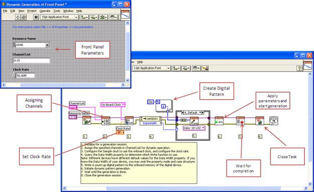
Figure 7 shows how to use the NI PXIe-6548 HSDIO stimulus-response instrument for the generation of a 1,000-sample, 16-bit waveform toggling at every clock edge.
Figure 7: Generating a Digital Pattern Using the NI-HSDIO API in LabVIEW
Programmable FPGA
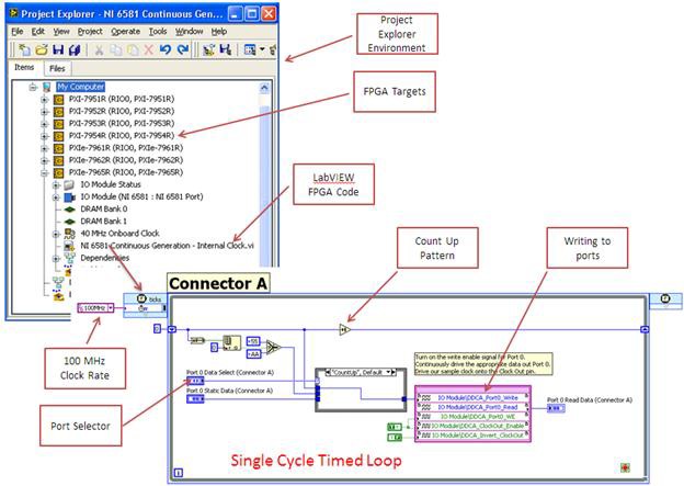
Figure 8 shows how to use the NI 6581 digital adapter module for NI FlexRIO to generate a simple digital pattern on 16 bits at a clock rate of 100 MHz. Engineers can pick the FPGA target from the LabVIEW Project Explorer as well as define a host VI that runs on the PC and an FPGA VI that runs on the target FPGA. DMA calls from the host VI to the target FPGA VI control the transfer of data to and from the host and FPGA target. Engineers also can use FIFOs and DRAM on the FPGA target to store data that is collected or needs to be generated, thus nearly eliminating the DMA transfer constraints such as latency and bandwidth.
Figure 8: Generating a Digital Pattern with NI FlexRIO Using NI LabVIEW
Note: Please see NI 6581 shipping examples for complete codes.
Multiple Options for Digital Test
NI HSDIO and programmable FPGA digital instruments satisfy two very distinct sets of requirements. NI HSDIO devices are ideal for instrument-like performance during which engineers might need to tweak physical parameters such as timing or voltage (for example, in a characterization lab). With programmable FPGA-based instruments, engineers can import existing HDL IP, implement custom tests (such as bit error injection), and emulate protocols – all in a flexible and reconfigurable manner. Engineers should expect better physical specifications from NI HSDIO devices such as eye diagrams and channel-to-channel skew and jitter, among other parameters. And they should expect higher flexibility, IP integration capabilities, and protocol emulation capabilities from a programmable FPGA -based digital instrument.
