Simulation of Integrated Power Controllers from ON Semiconductor
Overview
Contents
Introduction
NI Multisim is a powerful tool used to simulate and prototype power electronics of different ratings at early stages in the design flow. Engineers benefit from adding simulation to their approach especially if they have access to accurate models of AC/DC converters, switch-mode power supplies, and power controllers from leading semiconductor manufacturers. National Instruments works directly with semiconductor manufacturers to ensure that all models are validated to ensure simulation accuracy.
The simulation capabilities in Multisim enables circuit performance evaluation including critical characterization of DC ripples, transient responses, switching and conduction losses. By addressing or reviewing such data, an engineer can reduce the number of design iterations.
This application note analyzes two example designs of an isolated 2 W bias supply circuit and a 12 V forward converter based on power supply controller parts from ON Semiconductor. This simulation approach in NI Multisim lead to an approach to optimize design performance of these circuits.
2W Isolated Bias Supply
In this application we begin with a circuit that is a 2W bias supply that steps down an input range of 36 V to 78 V with an output of 12 V. This application is widely used in automotive circuits as well as telecommunications systems.
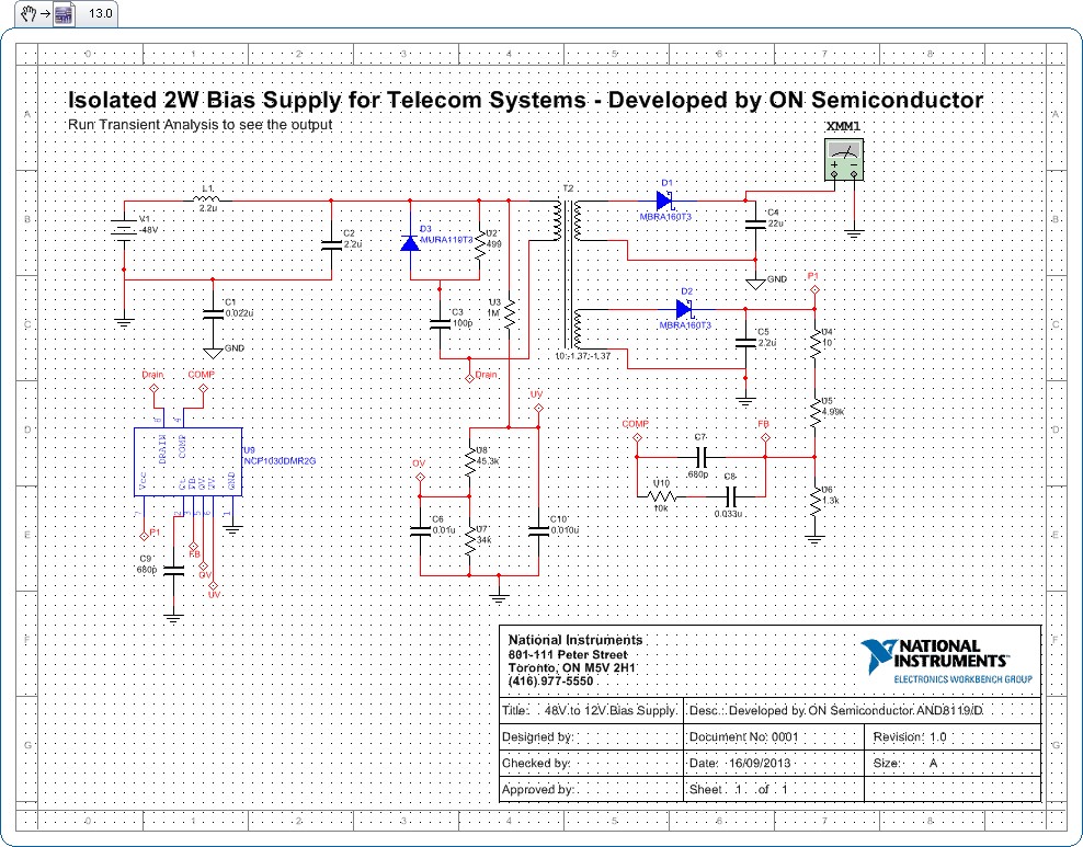
The circuit design is based on the NCP1030 device developed by ON Semiconductor, which is a highly integrated power switch circuit. The part symbol, model, and footprint are available in Multisim, and the theoretical background and design steps are explained in detail in ON Semiconductor application note AND8119/D.
The circuit schematic in the Multisim snippet (a PNG image that you can drag and drop into Multisim to directly load the design) shows the layout that includes new components of nonideal RLC models, rectifiers, and configurable transformers.
Figure 1: 48 V to 12 V Bias Supply in Multisim (drag and drop into Multisim to load the design)
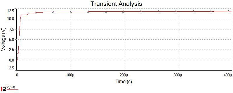
The transient analysis of the design results is shown in below.
Figure 2: Transient Analysis Results of the 48 V to 12 V Bias Supply in Multisim
The transient response shows a buildup time of around 10 µs for the regulated voltage to stabilize at 12 V. The RLC components used in this circuit model the non-ideal and parasitic effects associated withthe impedances. The switching controller is based on the SPICE model provided by ON Semiconductor. Once you have accurately evaluated the design of such a circuit using Multisim you will have high confidence it will perform to the desired specifications.
A Simple 12V, 22W Offline Forward Converter
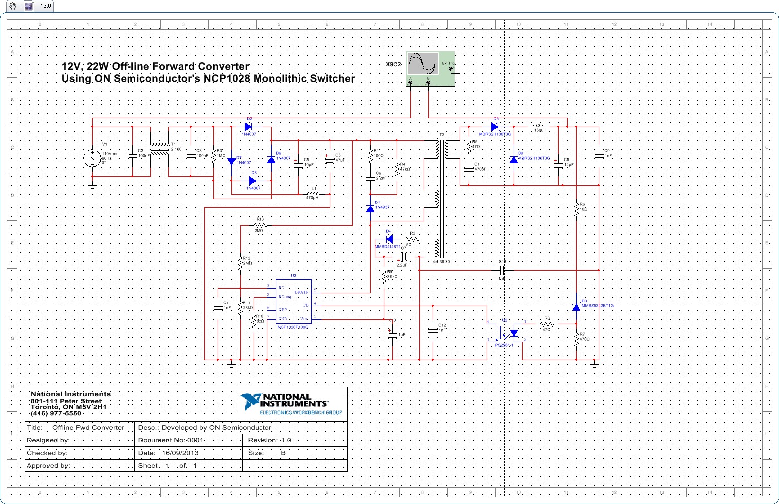
This forward converter developed by ON Semiconductor is based on the NCP1028 controller, available in the Multisim database. NCP1028 is a high-voltage switching regulator for medium power offline switched-mode power supplies (SMPSs). This circuit provides 12 V output up to 2 A peak output current over the entire universal input range (90 to 265 VAC). This performance makes it suitable for almost any application that involves power supply design.
You can learn more about the technical design details in ON Semiconductor application note AND8489/D.
The following models of power components in Multisim were used in the design:
- Configurable transformers
- Diode rectifiers
- Nonideal RLCs
- Optocouplers
- NCP1028 controllers
Figure 3 is a snippet of the design.
Figure 3: 12 V AC to DC Forward Converter Schematic
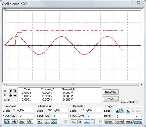
An alternative way of learning about the transient response of this circuit is by running an interactive simulation. This allows you to vary the value of different interactive components (for example potentiometers etc…) on the schematic and viewing how the response is affected while the simulation is running. Different response types could be evaluated using different instruments such as the oscilloscope, the bode plotter, or the DMM.
Figure 4: Measured Transient Response on the Built-In Virtual Oscilloscope Instrument of Multisim
As the above oscilloscope measurement shows, an AC input voltage of 180 V peak amplitude is regulated to a DC level of 12 V. The setting time of this regulator circuit is less than 10 ms. You can perform further advanced analyses to evaluate the ripple level of the DC output, the efficiency of the circuit, and the sensitivity of the circuit to parametric variations. The non-ideal RLC and the configurable transformers help to accurately model all of the parasitic effects while the SPICE model of the switching control provided by ON Semiconductor almost guarantees the alignment of this simulation with a fabricated physical prototype.
Conclusion
NI partners with leading semiconductor manufacturers to offer circuit designers a complete library of accurate component models and a simulation environment that enables them to evaluate circuit performance, explore various parameters that are critical in design decisions, meet specifications and ultimately reduce the number of prototype iterations.
- Download a 30 day free evaluation of Multisim
- Read about 11 Ways to Prototype Faster with NI Multisim


