Optimizing your LabVIEW FPGA VIs: Parallel Execution and Pipelining
Overview
Using the LabVIEW FPGA module, you can create customized I/O according to the specific requirements of your application. The pipelining and parallel code execution techniques described in this document allow you to optimize the performance for your FPGA code
Contents
- Optimizing for Speed
- Parallel Execution
- Pipelining
- Loop Rate vs. Latency
- Benchmarking
- Single Cycle Timed Loop
- Additional Resources
Optimizing for Speed
Using the LabVIEW FPGA module, developers can implement a wide variety of data acquisition and processing routines that run on FPGA targets such as RIO and CompactRIO devices. Hardware execution provides greater performance and determinism than most processor-based software solutions. Once the code is compiled and running on the FPGA it will run without the jitter associated with software execution and thread prioritization typical to most common operating system and even present to a much smaller degree in real-time operating systems.
LabVIEW's graphical programming methodology is inherently parallel in nature and lends itself to designing highly parallel code. On a CPU based target such as Windows the graphical code is scheduled into serial program execution where all functions and operation are handled sequentially on the processor. The LabVIEW scheduler takes care of managing multiple loops, timing, priorities and other settings that determine when each function is executed. This sequential operation causes timing interaction between different parts of an application and creates jitter in program execution.
On an FPGA-based target, each application process (subset of the application that you define) is implemented within a loop structure. The LabVIEW diagram is mapped to the FPGA gates and slices so that parallel loops in the block diagram are implemented on different sections of the FPGA fabric. This allows all processes to run simultaneously (in parallel). The timing of each process is independent of the rest of the diagram, which eliminates jitter. This also means that you can add additional loops without affecting the performance of previously-implemented processes. You can add operations that enable interaction between loops for synchronization or exchanging data.
While LabVIEW FPGA offers an ideal platform for running high-speed deterministic code, you may still encounter situations where process loop times need to be optimized further. This application note describes several techniques we can use to take full advantage of the parallel nature of the FPGA execution model in these situations.
Parallel Execution
Using the parallel nature of graphical programming and the truly parallel implementation of the LabVIEW diagram on the FPGA, you can further optimize execution speed by partitioning your application code into smaller processes. This enables each process to achieve a higher loop rate and an overall higher execution rate for the application than if the entire application was running in one loop.
For example, a typical DAQ application can be partitioned into processes for data acquisition, data processing, and data transfer to a host application. These tasks could be implemented as a sequence in a single loop, but could also be coded as three separate loops as shown below. One loop handles data acquisition and timing of the acquisition, and passes data off to processing. The second loop receives data from the first loop, processes it, and passes it off to the third loop, which handles the transfer of processed data to the host application.
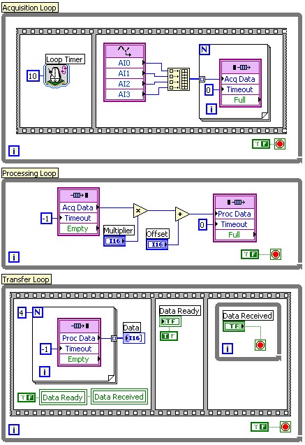
Figure 1: Example of a three loop application using FPGA FIFOs to pass data between the different loops
Data transfer and synchronization between parallel loops or code segments can be handled using standard LabVIEW FPGA tools including FIFOs and occurrences. FIFOs allow you to store and buffer data in your FPGA application, so they are useful for passing data between two different parts of the block diagram or to subVIs. They can also be used to synchronize two different loops such that the receiving loop is synchronized with the sender based on the data it receives. Multiple FIFOs can be created in a FPGA VI and each FIFO can be configured with an individual data type and depth. FIFOs configured for block memory share the user memory available on the FPGA and do not use up any of the FPGA gates themselves. Using the Timeout parameter on the FIFO Read and Write nodes you can configure the individual behavior of these nodes.
If synchronization is required between two loops that do not exchange data directly, you can use occurrences. An occurrence allows you to block one loop using the Wait for Occurrence function until another loop has completed a specific operation and calls the Set Occurrence function, as is shown in the following diagram.
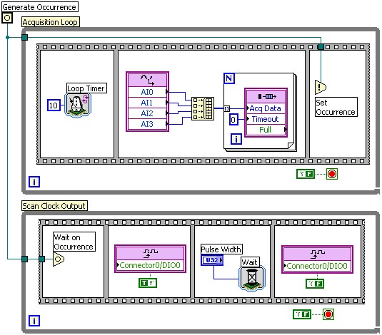
Figure 2: Example of using an occurrence to synchronize one loop to another
This technique can be applied to almost any application. By looking at the data flow within your application, you can identify different processes that can run independently of each other even if they need to be synchronized in the larger scheme of the application.
In addition to improving performance, this modular programming approach helps you to organize and manage your application code, allowing you to more easily test and debug your application and improve code reuse in future applications that have similar requirements.
Pipelining
Pipelining is an extension of parallel code execution concept that works within a single process. Instead of partitioning the process, you can use pipelining to achieve parallel code execution by partitioning the code sequence into smaller segments that execute over multiple iterations of the loop. As with parallel loops, the smaller code segments run in parallel in the same loop. By reducing the length of the critical path (longest code segment) in each loop iteration, you decrease the loop execution time.
The following diagram illustrates how a process consisting of A and B code segments can be pipelined to reduce the length of each loop iteration. Passing data from one loop iteration to the next (from A to B) is easily implemented using the shift register..
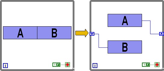
Figure 3: Illustration of pipelining in a LabVIEW While loop
One type of application that can take advantage of pipelining is data acquisition with preliminary data processing. In the following example, a digital input line is sampled and the width of all pulses in the digital signal is measured and written to a FIFO for processing in a separate loop. In both implementations, a shift register is used to store the state of the digital line and a timestamp for the last signal edge to support change detection and calculation of the time between consecutive signal edges.
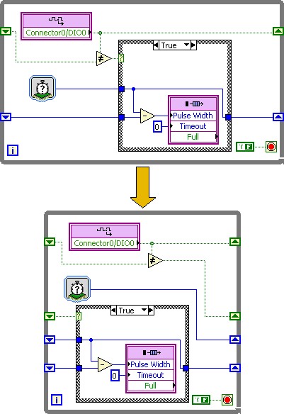
Figure 4: Example of a LabVIEW application without pipelining
on top and with pipelining on the bottom
In the top implementation (without pipelining) the loop continues to calculate the pulse width (subtraction) and writes the value to the FIFO when an edge is detected.
In the bottom implementation (with pipelining), when a signal edge is detected a Boolean flag is written to an additional shift register so that in the next loop iteration the pulse width is calculated and written to the FIFO. At the same time the next sample is acquired from the digital input and compared to the previous sample. This allows the bottom loop to detect edges and process them in parallel and run at a higher loop rate, thereby enabling it to detect shorter pulses and have better timing resolution in the pulse width measurement.
Loop Rate vs. Latency
When considering pipelining for optimizing your code, we must be aware of the various application performance requirements. The first and most obvious performance consideration is the loop rate or loop period. Often we are most interested in increasing the loop rate to improve the responsiveness or throughput of the system.
In some applications, however, latency is the more important consideration. Latency is simply the delay between two points in code execution, and is normally associated with control applications where system performance is determined by the time delay between an input signal measurement and the corresponding control signal output after some processing (e.g. PID algorithm) has been applied to the input data. To improve or optimize a control application we commonly want to decrease the latency to achieve tighter control over our process.
By applying the pipelining technique to a typical control loop implementation, we can increase the loop rate significantly, because (for most FPGA control applications) the two most time-consuming functions are analog input and output operations. The data processing is typically a relatively short operation. By pipelining the input and output operations and placing them in parallel in the loop, we could effectively reduce the loop period to the duration of the longer of the two operations.
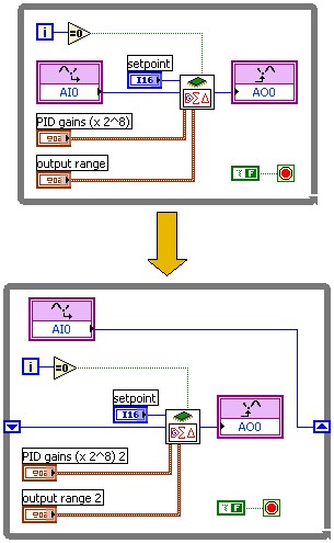
Figure 5: Applying pipelining to a typical control loop application using a PID algorithm
However, when we measure the latency of the control sequence (input/processing/output) with pipelining, we will see that we in fact have slightly increased the latency compared to the non-pipelined implementation. The latency can not be decreased because we always need to run through each of the three components of the control loop - input, processing, and output. By passing data through the shift register of the loop we have added one iteration of the loop overhead, increasing the latency. In the example above the non-pipelined implementation has a loop period of 221 clock cycles (5.5 microseconds, 181 kHz). The pipelined implementation has a loop period of 172 clock cycles (4.3 microseconds, 232 kHz), However the latency of the control loop is increased by a couple of clock cycles due to the loop overhead.
This behavior is generally true anytime we use pipelining to improve the loop rate. We must be aware of this effect and understand which of these two performance measurements, loop rate or latency, is more important in optimizing our application.
Benchmarking
As you optimize your application, you can measure the effect of different programming techniques using the timing functions in LabVIEW FPGA. You can easily add small code segments to measure performance information such as loop execution time and latency. Because these timing functions are also implemented in parallel on the FPGA they do not affect the performance of the application, so you can measure the true performance of your system.
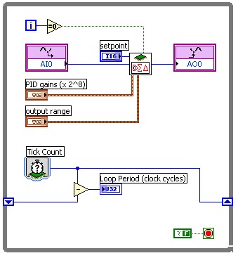
Figure 6: Benchmarking a closed loop control PID algorithm
The example above shows the most common technique for measuring the loop period of a typical process. The tick count function returns the current value of the FPGA clock, which we can use to calculate the time difference between consecutive loop iterations. For added flexibility, the timing functions in LabVIEW FPGA can be configured to operate in units of FPGA clock cycles (ticks), microseconds, or milliseconds.
Single Cycle Timed Loop
Another tool for optimizing your application for speed and FPGA usage is the single cycle timed loop (SCTL). The SCTL is an advanced programming structure available in LabVIEW FPGA. LabVIEW code placed inside the SCTL is more highly optimized when it is compiled for the FPGA, generating a smaller foot print and running more efficiently. As the name indicates, code inside the SCTL runs in a single cycle of the FPGA clock. Due to this behavior there are some significant restrictions on the code that you can place inside an SCTL - some operations are inherently multi-cycle, and can't be used. A detailed discussion of the SCTL is beyond the scope of this document, but more information on the SCTL and how to use it can be found in the LabVIEW FPGA manual.