Digital States, Voltage Levels, and Logic Families
Overview
Learn about digital states, voltage logic levels, and logic level families for digital signals. This tutorial is part of the Instrument Fundamentals series.
Contents
Digital States
In digital devices, there are only two states: on and off. Using only these two states, devices can communicate a great deal of data and control various other devices. In binary, these states are represented as a 1 or 0. Binary 1 is typically considered a logic high, and 0 is a logic low.
Voltage Levels
Digital devices, however, are often driven by analog devices with an infinite number of states. How do you turn an infinite number of states into only two? The answer is by creating voltage logic levels, which define the voltage to represent a logic high or logic low.
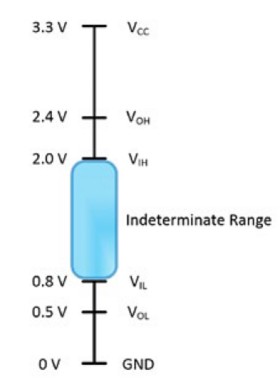
Figure 1: Voltage levels define the analog voltage that represents a logic high or low.
A system can define the voltage logic levels at any value it chooses, but many circuits represent a logic high by +5 V or +3.3 V to ground and a logic low as ground or 0 V. This type of system is called a positive or active-high. It describes how the pin is activated—for an active-high pin, you connect it to your high voltage.
A negative or active-low system is the reverse. The higher voltage represents a logic low and the lower voltage represents a logic high. For an active-low pin, you must pull that pin low by connecting it to ground. Data sheets often denote a pin is active-low by putting a line above the pin name, such as EN.
Although a high and low are specified, in most systems there is actually a range so as to be more practical. For example, a logic high might be any value between 2 V and 5 V and a low might be any value from 0 V to 1 V. Voltages outside those ranges are considered invalid and occur only in a fault condition or during a logic-level transition.
Z and X States
Although a digital signal can have only two states—on and off—you can use additional states to assist with acquiring and generating digital signals. With tristate logic, there is a third possible condition: a high-impedance state where the output is disconnected from the line. This state isn’t a high or low, but rather a floating or high-impedance state. It has the designation Z and is often used as an enable line.
The most common use of the Z state is to test one or more digital lines that can be driven by multiple transmitters. The data port on a memory chip is a good example of this. When the computer writes into the memory device, the computer needs to drive the data to be written into the memory chip on the data pins of the memory device (either 0 or 1). Later, when the computer processor needs to read out the contents of the memory, the memory device needs to drive the previously stored data value back to the computer processor (usually a Z state on the data pins).
A fourth state you might see is the hold state that is designated with an X. When generating digital signals, you might find it useful to have the device simply maintain the channel at its current state, regardless of which state that might be. This state is useful when setting initial or idle states.
When you acquire data, the X state has a different designation of don’t care. This state is useful when you are comparing an acquired digital signal to an expected signal. For instance, on a signal you may care about only the first four values in a 10-value signal. You can use the X state for the last six values and compare just the first four.
| State | Designation |
|---|---|
| 0 | Logic Low |
| 1 | Logic High |
| Z | High Impedance |
| X | Hold State or Don´t Care |
Table 1: A digital signal can be in only a high or low state; however, the Z and X states can assist in applications that generate or acquire digital signals.
Logic Families
Standardized logic families make it easier to work with circuits and components. They provide a standardized voltage level that constitutes a logic high or logic low. All circuits within a logic family are compatible with other circuits within that same family because they share the same characteristics.
Single-Ended Logic Families
Single-ended logic families specify voltage levels in relation to ground. The four levels are defined as:
- VOH (output high-level voltage) – This is also known as the generation voltage high level. When configured for active drive generation, this is the voltage produced by the device when it generates a logic high. When configured for open collector generation, this is the equivalent to setting the data channel to a high-impedance state.
- VOL (output low-level voltage) – This is also known as the generation voltage low level. This is the voltage produced by the device when it generates a logic low.
- VIH (input high-level voltage) – This is also known as the acquisition voltage high level. This is the voltage level necessary to send to the device for it to read a logic high.
- VIL (input low-level voltage) – This is also known as the acquisition voltage low level. This is the voltage level necessary to send to the device for it to read a logic low.
Figure 2: Single-ended logic levels are specified for output and input.
To accurately communicate with a device, be sure to configure the digital device such that the following conditions are met:
- VOH ≥ DUT VIH
- VOL ≤ DUT VIL
- VIH ≤ DUT VOH
- VIL ≥ DUT VOL
- VIH > VIL
There is usually a cushion between the output voltage of one device and the input of another. This is referred to as the noise margin or the noise immunity level (NIM). If you are in a noisy environment and having difficulty with incorrect data bits, consider increasing this value.
There are several single-ended logic families. Transistor-transistor logic (TTL) is very common for integrated circuits and is used in many applications such as computers, consumer electronics, and test equipment. Circuits built from bipolar transistors achieve switching and maintain logic states. A TTL must also meet specific current specifications and rise/fall times, which you can read more about in What Is the Definition of a TTL-Compatible Signal?.
Figure 3: Standard 5 V TTL Voltage Levels
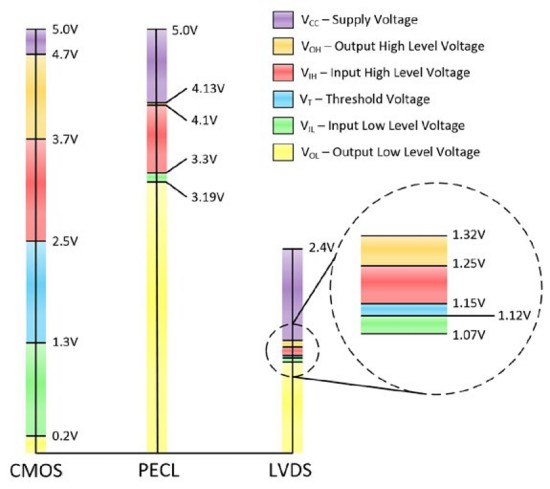
Another common IC family is CMOS. These devices have high noise immunity, require less power consumption, and have a lower based voltage. Most of the voltage levels are similar to TTL devices for greater compatibility. This makes it easy to switch from a TTL to a CMOS device, but going the other direction can be trickier. Too high a voltage to a CMOS could damage the chip. In this case, you can use a voltage divider to reduce the voltage.
Figure 4: Standard CMOS Voltage Levels
Differential Logic Families
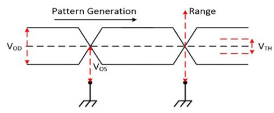
Single-ended logic families use a set voltage level in relation to ground; however, differential logic families use the difference between two values and not a reference to ground. For the differential signal to be interpreted as a logic low, the signal must be less than its complementary signal by more than a particular value known as the threshold value (VTH). Because the signals are referenced and transmitted together, you can achieve higher noise immunity in your signals than using single-ended logic families. Voltage levels for differential logic families are typically specified from a differential rather than an absolute voltage. The four levels are defined as:
- VOD (output differential voltage) – This is the difference in voltage between the signals.
- VOS (offset voltage) – This is the common mode of the differential signal. Think of this as the average of the two signals. It is a reference to ground.
- VTH (threshold voltage) – This is the difference in voltage needed for the device to register a valid logic state.
- VRANGE (input voltage range) – This is the absolute voltage referenced from ground allowed by the device.
Summary
- A voltage logic level defines the voltage to represent a logic high or a logic low.
- Many circuits represent a logic high by +5 V or +3.3 V to ground and a logic low as ground or 0 V. This type of system is called a positive or active-high.
- In tristate logic, the Z state is a high-impedance state and is often used as an enable line.
- In digital generation, the X state maintains the current logic level. In digital acquisition, it indicates a don’t care state.
- Logic families provide a standardized voltage level that constitutes a logic high or logic low.
- TTL is based on VCC = 5 V.
- CMOS is based on VCC = 3.3 V
- Differential logic families use the difference between two values and not a reference to ground.
- LVDS is a low-noise, low-power, and low-amplitude differential method with VCC = 3.3 V.
- LVPECL circuits are a type of ECL circuit that require a pair of signal lines for each channel (VCC = 3 or 3.3 V).


