Is Your Data Inaccurate Because of Instrumentation Amplifier Settling Time?
Contents
- Introduction
- What is Settling Time?
- How to Run Your Own Settling-Time Test
- What Affects Settling-Time
- Same ADC, Different Setting Time Characteristics
- About the NI-PGIA
- Reducing Settling-Time Effects
- Conclusion
Introduction
You may not be aware that the analog data you acquire may not accurately reflect the real-world signals you measure. For example, when you use a plug-in data acquisition (DAQ) board with a 12-bit resolution analog-to-digital converter (ADC) and scan 16 channels for input with a sampling rate of 100 kS/s, your acquired data may not be 12-bit accurate. The data that the DAQ board retrieves appears error free because no data was lost; however, the data retrieved may not be within the specified ADC accuracy. This is the result of instrumentation amplifier settling time, an important consideration when you use any plug-in DAQ board.
There are two ways to reduce inaccuracies caused by amplifier settling time:
- Select a DAQ board with an instrumentation amplifier that is guaranteed to settle at all sampling rates and gains.
- Reduce sampling rates.
What is Settling Time?
Settling time is the amount of time required for a signal that is being amplified to reach a certain accuracy and stay within the specified range of accuracy. To see how settling time affects a DAQ system, consider the block diagram in Figure 1. This block diagram shows the major components on a DAQ board that are necessary for acquiring analog data into a computer:
- A multiplexer (mux)
- An instrumentation amplifier
- A sampling ADC
- A first-in-first-out (FIFO) buffer

Figure 1. Major Components of a Plug-In DAQ Board
The real-world signals being measured are first routed from a particular channel via the multiplexer. The signals then enter the instrumentation amplifier. The instrumentation amplifier applies a specified amount of gain to an input signal, which raises the signal to a higher level and ensures proper A/D conversion. The amplifier also converts any differential input signals applied to the DAQ board to a single-ended output so that the ADC can correctly digitize the data. The ADC then samples and holds the signal until the signal is digitized and placed into the FIFO buffer on the board. In the FIFO, the digitized signal is ready to be transferred from the board to computer memory via the PC bus for further processing.
The time needed to amplify the signal to the higher level while maintaining the accuracy of the ADC – in other words, the settling time of the instrumentation amplifier – is a major concern when you use plug-in DAQ boards. The instrumentation amplifier must settle before the A/D conversion takes place or your data will be inaccurate. If the amplifier does not settle, the voltage digitized will be higher or lower than the actual voltage signal you attempted to acquire.
Settling time is the result of many factors in the instrumentation amplifier. Consider a standard resistance-capacitance (RC) lowpass filter circuit design. When you apply a voltage step to an RC circuit, the signal requires a certain amount of time to rise and settle within a percentage of the voltage you want, as seen in Figure 2. This percentage of V is the range of accuracy, and the time it takes for the signal to get within the specified range is the settling time.
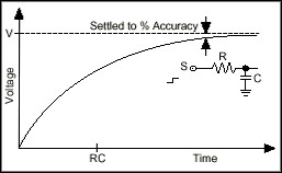
Figure 2. Settling Time of a Standard RC Circuit
Figure 3 shows the settling time characteristics of a standard instrumentation amplifier. Notice that the signal rises above the range, oscillates, and stabilizes within the acceptable range of accuracy. Again, the time it takes for the signal to get within the range of accuracy is the settling time.
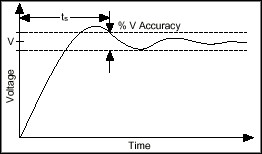
Figure 3. Settling Time of an Instrumentation Amplifier
To better understand the concept, compare amplifier settling time to the settling time of a spring-mass system. Figure 4a shows a spring with a mass hanging from it at rest. Figure 4b shows the spring stretched so that when the mass is released, as in Figure 4c, it begins to bounce. When the bouncing distance decreases to within a specified or acceptable range of the resting position, as in Figure 4d, the system is considered to have settled. The time from when the spring is released to when its bouncing decreases to the desired range of motion is the settling time.
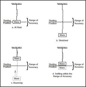
Figure 4. The Settling of a Spring-Mass System
Notice the similarity between the settling of a spring-mass system and amplifier settling time. When the amplifier applies gain and the signal is changed to the desired value, a period of time passes until the signal reaches and stays within the accepted range of accuracy. This time period is similar to the time the spring-mass system takes to decrease its bouncing to within the acceptable range.
How to Run Your Own Settling-Time Test
The following sections detail two methods for determining the settling time of your DAQ board – one with DC signals and one with AC signals.
DC Signal Settling-Time Test
Figure 5 shows the DC signal test, in which two DC signals are connected to the DAQ board. To run the test, connect a ± signal to channels 1 and 2, respectively. The input signals should be close to but not above the DAQ board full-scale input range when a high gain is applied. For example, a ±0.048 V input with a gain of 100 results in a 4.8 V signal, which is 0.2 V less than the full-scale value of the board. When running this test, it is important that you do not input a signal greater than or equal to the full-scale value because this can saturate the amplifier and result in a longer settling time. Next, complete at least a 100-point single-channel timed data acquisition for each channel and average the results to obtain a positive and a negative reference voltage. In Figure 5, these reference voltages are represented by the lines labeled VREF and -VREF.
After acquiring the reference values individually, acquire 100 points at the maximum sampling rate for the two channels, alternating the sampling between the channels; this is also called scanning the channels. Figure 5 shows these points as dots near the reference voltage lines.
Again, average the data; you will use this average to calculate the settling-time error at the maximum sampling rate. In Figure 5, the average of the positive data is 0.04 V; the average of the negative data is –0.048 V.
To calculate the error, compute the maximum deviation between the reference voltages and the positive and negative averages of the scanned data; in other words, subtract the averaged scanned data from the positive and negative reference voltages and use the maximum of the absolute values. This deviation is the amount of settling-time error in voltage at the maximum sampling rate. In the example in Figure 5, the positive and negative deviations are 0.01 V and –0.002 V respectively, which results in a maximum settling-time error of 0.01 V.
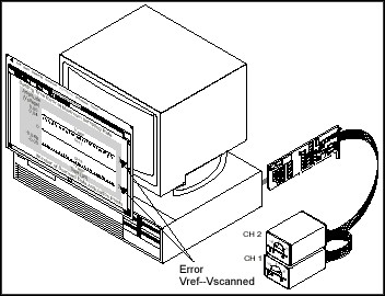
Figure 5. DC Signal Settling-Time Test
Repeat this process at different sampling rates and gains until the board settles to the specified accuracy. To plot the error in least-significant bits (LSBs) versus time, divide the absolute value of the maximum deviation by the voltage equal to 1 LSB for the gain you applied. For example, in Figure 5,
at a gain of 100. Therefore, the error of 0.01 V in Figure 5 equals 409.8 LSBs. Invert the sampling rate to calculate the settling time with that particular amount of error. At a sampling rate of 100 kS/s, for example, the settling time is 10µs. After the plot is complete, compare the plot to the specified board accuracy to see how long your board takes to settle to the specified accuracy.
AC Signal Settling-Time Test
Figure 6 shows the AC signal test. In Figure 6, a full-scale low-frequency AC signal is connected to channel 1, and channel 2 is connected to ground. By alternating the sampling between both channels (scanning) at the maximum sampling rate, as shown in the top graph in Figure 6, and performing a fast Fourier transform (FFT) on the data from channel 2, as shown in the bottom graph, you can see if the amplifier correctly settled.
If any large spikes appear in the FFT plot at the frequency of the channel 1 input signal, as in Figure 6, the amplifier did not settle completely. The magnitude of the spike is the amount of voltage error; the corresponding settling time is the inverse of the sampling rate. Notice that using an input signal that is too high in frequency could cause crosstalk, which would appear the same as a settling-time error in the channel 2 spectrum.
Note: Crosstalk is an expected natural phenomenon caused by the close proximity of signals and capacitance, which results in unwanted coupling of the signals. All DAQ boards have a measure of crosstalk.
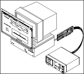
Figure 6. AC Signal Settling-Time Test
Repeat this process with different sampling rates and gains to see how quickly the amplifier settles and with what amount of error. When you have minimized the magnitude of the spike in the FFT plot, the amplifier has settled correctly. You can use this process to determine the sampling rate and gain at which you can acquire data accurately with your DAQ board.
What Affects Settling-Time
Gain, multiplexing, source output impedance, and transmission line resistance and capacitance all affect settling time. Gain and settling time typically have a direct relationship – during amplification, the instrumentation amplifier takes longer to settle at higher gains because of decreased bandwidth and higher signal resolution.
Multiplexing can cause settling time to increase when more than one channel is scanned. Rapid switching between multiple channels at different DC values results in a high frequency input to the instrument amplifier. An example of the instrument amplifier input during multiplexing is shown in Figure 7.
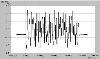
Figure 7. Input to Instrumentation Amplifier when Multiplexing 42 DC signals
The instrumentation amplifier requires time to settle once a voltage is applied to its input. If channels are switched and sampled at a rate faster than the settling time of the amplifier, inaccurate readings will results. This problem becomes more pronounced if the voltage difference between adjacent channels is large.
Multiplexing input channels with high source impedances results in longer amplifier settling times. The high impedance of the source combined with the charging and discharging from capacitances inherent in the multiplexer during switching can cause further inaccuracies when scanning multiple channels. As the current being discharged from the multiplexer seeks ground, the current passes through the high-impedance source; the current and the high-impedance source combine to produce a voltage. This voltage is added to the original signal and results in inaccurate data.
Transmission line effects also influence settling time when you use higher impedance sources. The charging associated with the capacitance in the cable increases the settling time of the system. The result of the cable capacitance is similar to having small lowpass filters in the cable that take time to charge and discharge, causing a decrease in the throughput of the signal.
Same ADC, Different Setting Time Characteristics
If you compare the performances of two DAQ boards that have the same resolution ADCs but different instrumentation amplifiers, you will notice the extreme variation that differences in settling times cause. Figures 8 and 9 show the results of the DC signal settling-time tests for two National Instruments multifunction plug-in DAQ boards – one board has an off-the-shelf instrumentation amplifier, and the other contains the NI-PGIA™. To create the graphs in Figures 8 and 9, ±0.048 V signals were input into channels 1 and 2 on each board at a gain of 100, and the sampling rates were adjusted to demonstrate the effects of settling time.
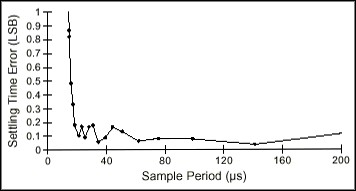
Figure 8. DC Settling-Time Test of a Board Using an Off-the-Shelf Instrumentation Amplifier
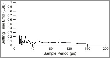
Figure 9. DC Settling-Time Test of a Board Using the NI-PGIA
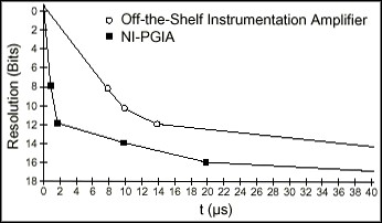
The low-cost board used to generate Figure 8 contains an off-the-shelf instrumentation amplifier, which the margin of error illustrates. The board took between 16 to 17 µs to settle to 0.5 LSB, the specified accuracy. The high-accuracy, high-performance board used to generate Figure 9 contains the NI-PGIA instrumentation amplifier, which National Instruments specifically designed for plug-in DAQ boards to solve settling time problems. Notice how much more quickly the NI-PGIA settles than the amplifier of the low-cost board.
Figure 10 compares the settling time of the NI-PGIA to a standard off-the-shelf instrumentation amplifier. The NI-PGIA settles to 12-bit accuracy approximately five times faster than the standard instrumentation amplifier, which the DC signal test also revealed.
Figure 10. Settling Time of the NI-PGIA Versus an Off-the-Shelf Instrumentation Amplifier
About the NI-PGIA
The NI-PGIA differs from standard off-the-shelf instrumentation amplifiers because the NI-PGIA is specially designed to settle to 12-bit accuracy within 2 µs. The high accuracy and low settling time of the NI-PGIA is due largely to the input operational amplifiers (op amps), which operate at close to a closed-loop gain of 1 regardless of the programmed gain. This differs from most operational amplifiers, which operate with an increasing closed-loop gain as the programmed gain increases.
The design of the NI-PGIA allows the bandwidth and linearity to stay relatively constant as the gain increases. Thus, the settling time remains within the 2 µs range even at the highest gain of 100. Nonlinearity is approximately 1.5 parts per million (ppm), and the gain error for the NI-PGIA is ±0.02%. The variation in gain error is due mostly to the ratio matching of the gain-setting resistors of the NI-PGIA. The primary function of the resistors is to set the NI-PGIA gain that is going to be applied to the input signal.
While the DC common-mode rejection ratio (CMRR) of most instrumentation amplifiers usually decreases as gain decreases, the DC CMRR of the NI-PGIA is nearly independent of the gain. As with most standard instrumentation amplifiers, the NI-PGIA AC CMRR exhibits low-gain degradation because of internal stray capacitance. The NI-PGIA uses a transconductance design that accurately converts differential input signals into single-ended signals, eliminates the need for well-matched resistors within the instrumentation amplifier, and contributes to the high accuracy of the NI-PGIA.
Reducing Settling-Time Effects
The most effective way to reduce settling time is to use a DAQ board with an instrumentation amplifier that is guaranteed to settle to the accuracy you need at all gains and rates. Because the instrumentation amplifier is where most settling-time delay occurs, select a board with a superior instrumentation amplifier to acquire the most accurate data. For example, the National Instruments AT-MIO-16F-5 and AT-MIO-64F-5 boards have the NI-PGIA and can sample at any gain without experiencing the effects of settling time if source impedances are kept low.
If you already have a DAQ board without a special instrumentation amplifier, there are a few other techniques you can use to reduce settling time effects on data acquisition. However, none of these techniques are as effective as using a board with an instrumentation amplifier that is guaranteed to settle to the accuracy you need at all rates and gains.
One technique for handling settling-time effects is to specially arrange the input signals according to whether you are using continuous or interval-channel scanning, as shown in Figure 11. Signal arrangement may not be possible in all of your applications, but consider this method initially.
To scan channels continuously as quickly as possible with the same amount of time elapsing between each channel, you should consider arranging the signals so that the voltage swing is constant between each channel. When it is time to sample the sequence of channels again, however, you must sample the first channel twice to give the amplifier time to settle. By repeating the first channel sample, the amplifier has the time necessary to compensate for the maximum swing in voltage.
Interval scanning involves scanning all the channels as quickly as possible, with a delay before you begin to sample the first channel again. This type of scanning allows for the largest voltage swing on the channels to occur between the last channel sampled and the repeat of the first channel sample, thus giving the amplifier time to settle without any extra requirements.
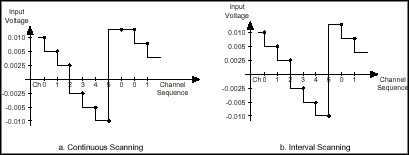
Figure 11. Signal Arrangement for Interval and Continuous Channel Scanning
Selecting the proper cabling material also helps reduce settling-time effects. Cabling is another consideration because of the capacitance that exists in cables. Avoid selecting cables with higher capacitances because of the delay time associated with charging and discharging. To reduce the amount of capacitance in a cable, keep the cable length as short as possible and select cables made of a naturally low-capacitance dielectric material such as polypropylene.
A final technique you can use to lower settling-time effects is to reduce the sampling rate and to select sources that have low output impedances. Reducing the sampling rate gives the instrumentation amplifier the time to settle to the accuracy you want. However, if you reduce the sampling rate to less than two times the maximum input frequency, an undersampled waveform and inaccurate data results.
When you are unable to use a device with a low output impedance, you can use a signal conditioning module or amplifier with a low output impedance that acts as a buffer to the board input. With this buffer, commonly referred to as a unity-gain buffer or a voltage follower, the multiplexer can receive low-impedance signals from high-impedance sources, thus reducing the effects of settling time.
When the amplifier does not settle fast enough for your frequency requirements, you need to consider selecting another DAQ board that settles at the sampling rate you need.
Conclusion
Selecting the proper DAQ board with regards to settling time consists of a few key issues. First, determine the maximum sampling rate and gains your application requires; you must select a DAQ board that settles to within your specifications. If you already have a DAQ board, run the DC or AC settling-time test to determine the settling time for your board.
After you know the constraints of your DAQ board, consider the output impedance of your signals and arrange your signals if possible to minimize the swing in voltages between channels. Finally, select cables that are as short as possible with low resistance and capacitance. Using these guidelines, you can resolve all of your settling time concerns and be confident that your acquired data is accurate.
