Benefits of Delta-Sigma Analog-to-Digital Conversion
Overview
National Instruments designed 24-bit delta-sigma analog-to-digital converters (ADCs) into many of their high-performance data acquisition (DAQ) devices, including the NI SC Express family, which includes integrated signal conditioning for directly measuring sensors. This allows high-resolution measurements with maximum accuracy, due to the delta-sigma ADC noise shaping and filtering. This paper explains the delta-sigma ADC architecture and the SC Express approach to automatically compensating for filter delays in software.
Contents
- Delta-Sigma ADC Architecture
- What Differentiates Delta-Sigma from Other Converter Technologies?
- NI Data Acquisition Hardware Based on Delta-Sigma Converters
- Delta-Sigma ADCs Improve Measurement Performance
Delta-Sigma ADC Architecture
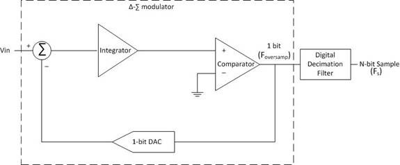
The hardware architecture of a delta-sigma (also referred to as sigma-delta) ADC consists of an integrator, a comparator, and a 1-bit digital-to-analog converter (DAC) arranged in a negative-feedback loop, as shown in Figure 1. An integrator circuit is fed the sum of the input signal and the negated output of the DAC. The output of the integrator is a ramp signal whose slope is proportional to its input. The integrator output is compared against the comparator reference signal to generate a 0 or 1. The binary output of the comparator is clocked into the digital decimation filter on every edge of the ADC oversample clock Foversamp. Each bit represents the direction of the ramp output of the integrator with respect to the comparator reference and, after multiple iterations, the bit stream resembles the quantized value of the input signal. Essentially, the feedback loop works such that the average output of the DAC matches the input signal. The digital decimation filter averages the bit stream to output an n-bit sample at the desired sample rate Fs.
Figure 1: A delta-sigma (Δ -∑ ) ADC consists of an integrator, a comparator, and a 1-bit DAC.
What Differentiates Delta-Sigma from Other Converter Technologies?
The differentiating aspects of delta-sigma ADCs are the use of oversampling in conjunction with decimation filtering, and quantization noise shaping.
Oversampling
Delta-sigma ADCs use sample rates that are large multiples, such as 128 times the Nyquist rate of a given signal, for instance. For example, to sample a 25 kHz signal, a sample rate greater than the Nyquist rate (above 50 kHz) would be sufficient. However, a delta-sigma ADC using an oversample rate of 128 will sample the signal at a much higher frequency than the Nyquist rate. This approach has several benefits, such as better anti-aliasing and higher resolution.
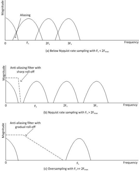
In the frequency domain, sampling a signal effectively modulates the input signal spectrum with carrier frequencies that are multiples of the sample rate Fs (that is, 0, Fs, 2Fs, 3 Fs, and so on). To ensure that these modulated versions of the input signal spectrum do not overlap, thus causing aliasing, the sample rate has to be greater than twice the maximum frequency component of the signal (that is, 2Fmax), the Nyquist rate. Conversely, if the input signal has frequency components above Fs /2, also called the Nyquist frequency, these components may alias into the sub-Nyquist frequency range, making it hard to detect signals of interest from among the aliases. This aliasing effect manifests as noise and signal distortion.
To prevent aliasing, the analog frontend of a data acquisition device often uses an analog lowpass filter that attenuates frequency components greater than the Nyquist frequency, prior to sampling by the ADC. There are stringent requirements on such filters as they are expected to have brick wall-like characteristics, which include sharp roll-off, flat passband, and so on. With such tight constraints and the fact that they have to be implemented as analog circuitry, these filters are complex to design and expensive to manufacture.
Figure 2: Oversampling relaxes the requirements on an analog antialiasing filter.
Delta-sigma ADCs relax the requirements on analog antialiasing filters by oversampling the input signal, as shown in Figure 2. Through oversampling, the modulated versions of the input signal spectrum are further separated in the frequency domain allowing for gradual roll-off filter characteristics, which make the analog antialiasing filter construction much simpler. Delta-sigma ADCs are composed mainly of digital components, making them even more attractive. With a primarily digital construction, they can be implemented in silicon and thus take advantage of advancements in very-large-scale integration VLSI technology.
Digital Decimation Filtering
The bit stream from the delta-sigma modulator is output to a digital decimation filter that averages and downsamples, thus producing an n-bit sample at the desired sample rate, Fs. This process of averaging has the effect of lowpass filtering the signal in the frequency domain, which attenuates the quantization noise and removes aliases from the band of interest. This decimation filter is usually built for an extremely flat frequency response in the passband and no phase error, a sharp roll-off near the cutoff frequency (about 0.49 times the sample rate Fs) and excellent rejection in the stop band, making it very effective at antialiasing. A digital decimation filter is typically implemented as a Finite Impulse Response (FIR) filter, such as a comb filter, which is a cost-effective way of implementing decimation.
Quantization Noise Shaping
The conversion of an analog signal into a digital signal introduces noise in the signal, which is called quantization noise. For a single digital sample, the noise is simply ± 1/2 LSB. The smaller the LSB, the higher the resolution of the ADC will be. A higher resolution implies lower quantization noise or a higher signal-to-noise ratio (SNR). The classical equation that captures the relation between ADC resolution and SNR is seen in Equation 1, where N is the effective number of bits of resolution of the ADC.
SNR = 6.02N + 1.76 dB (Equation 1)
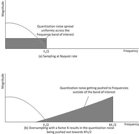
However, that is not the end of the story. A delta-sigma modulator behaves as a lowpass filter for the signal and a highpass filter for the quantization noise, thus pushing the noise to higher frequency regions, as shown in Figure 3. This phenomenon is called quantization noise shaping, and is taken advantage of by employing digital decimation that effectively lowpass filters the modulator output and removes the quantization noise. The reduction of noise power in the frequency band of interest means a higher SNR or a greater dynamic range, as the noise floor has been significantly lowered.
This improvement in SNR due to oversampling can be seen in Equation 2, where Fs is the sample rate, K is the oversample factor, and BW is the bandwidth of the input signal. This increase in SNR results in a larger effective number of bits of ADC resolution.
SNR = 6.02N + 1.76 + 10log (KFs /2BW) dB (Equation 2)
Figure 3 illustrates quantization noise shaping, which is one of the key advantages of delta-sigma ADCs.
Figure 3: Oversampling results in quantization noise shaping.
NI Data Acquisition Hardware Based on Delta-Sigma Converters
National Instruments designed 24-bit delta-sigma ADCs into many of their high-performance DAQ devices (SC Express, PXI/PXIe dynamic signal acquisition (DSA) devices, and NI C Series) that have integrated signal conditioning for directly measuring sensors. This allows high-resolution measurements with maximum accuracy, due to noise shaping and filtering.
In the SC Express family, NI PXIe-433x bridge input modules use 24-bit delta-sigma ADCs to perform simultaneously sampled, highly accurate strain gage- and Wheatstone bridge-based measurements. These devices are commonly used for strain, load, and pressure measurements in structural testing applications. NI PXIe-4353 takes advantage of 24-bit delta-sigma ADCs to make multiplexed precision thermocouple measurements. The thermocouple module is used in a wide variety of applications with varying sizes, as well as high-channel-count data acquisition systems for applications, such as temperature chamber monitoring
The DSA family of products, namely NI PXI/PXIe-446x, PXI-447x, PXIe-448x, PXI/PXIe-449x, and USB-443x, employ high-performance 24-bit delta-sigma ADCs. Applications of these devices include audio signal analysis, acoustics, vibration and modal analysis, and essentially any application that requires simultaneous sampling, large dynamic range (about 110 dB), and wide alias-free bandwidth (DC to about 0.45 times the sample rate, Fs).
Many C Series modules also use 24-bit delta-sigma ADCs to make highly accurate measurements for a variety of applications including thermocouple (NI 9211, 9212, 9213), RTD (NI 9217), high voltage and current (NI 9225, 9227, 9229, 9239, 9242, 9244), DSA (NI 9232, 9234), bridge-based measurements (NI 9235, 9236, 9237), and universal (NI 9219).
Compensation for Digital Filter Delay
Unlike other converter technologies, delta-sigma ADCs are free-running, meaning the input signal to the ADC is continuously being sampled even before a trigger condition happens. Moreover, because of the digital decimation filtering process, there is a delay before the input signal is converted to a digital sample. This delay is specified as the number of samples that the input signal acquired before the trigger was received. This delay may or may not have to be compensated for, depending on whether you are using a digital or analog trigger.
To simplify the process of acquiring data from NI devices using delta-sigma ADCs and correlating that data with data from other modules, several NI DSA and SC Express devices compensate for this group delay.
- The sample clock output is generated at the point in time when the input signal is valid at the ADC input pins. When acquiring data, the most NI DSA and SC Express devices generates a sample clock, then waits for the data associated with that sample clock to be acquired, then returns that data. As a result, any other acquisitions timed with this sample clock line up with the returned data.
- Any triggers generated or received are interpreted based on their relationship to the sample clock being generated. For example, a start trigger that starts an acquisition results in data from the next sample clock being returned as the first point in the acquisition.
- Several NI DSA and SC Express devices have a filter delay removal feature which automatically discards filter delay samples. Refer to the Filter Delay Removal topic in the DAQmx Help for details on hardware that supports this feature.
These software considerations make it easier for you to synchronize NI DSA and SC Express hardware with other devices with no extra programming. Refer to device specific product documentation for more information.
Delta-Sigma ADCs Improve Measurement Performance
Delta-sigma ADCs implement oversampling, decimation filtering, and quantization noise shaping to achieve high resolution and excellent antialiasing filtering. Many SC Express, DSA, and C Series sensor measurement devices from National Instruments take advantage of 24-bit delta-sigma ADCs for high-performance measurements.


