Creating FPGA-Based I/O Personalities for NI VeriStand
Overview
Contents
- What Are FPGA-Based I/O Interfaces?
- Why Use FPGAs for Real-Time Test Applications?
- How Custom FPGA Personalities Work With NI VeriStand
- NI VeriStand FPGA Personality Architecture
- Next Steps
What Are FPGA-Based I/O Interfaces?
Field-programmable gate arrays (FPGAs) are reprogrammable silicon chips that provide the superior execution and reliability benefits of hardware logic implementations such as those found in application-specific integrated circuits (ASICs), with the added flexibility of software- or firmware-based implementations. Using configurable logic blocks and programmable routing resources, you can configure FPGAs to implement custom hardware functionality without ever physically modifying the device. Instead, you develop digital computing tasks in software and compile them to a bitstream file that contains information on how the FPGA’s logic and routing components should be configured and connected.
Why Use FPGAs for Real-Time Test Applications?
With user-defined FPGA-based I/O interfaces, you can create custom I/O devices that can implement a combination of signal processing, simulation, triggering, and control tasks to produce an I/O interface that exactly meets your application needs. Additionally, because the I/O interface is FPGA-based, you can easily reconfigure the personality or behavior of the interface to adapt to new requirements or to create test systems capable of being used for multiple applications without changing hardware setups.
Customizable I/O is one of the most common reasons to use FPGAs in a real-time test application. You can choose from more than 100 C Series signal conditioning modules to provide specialized interfaces for your application. By combining this variety of signal conditioning options with the flexibility of FPGA-based I/O devices, you can quickly create I/O interfaces with custom timing and triggering capabilities that exactly meet your real-time testing application requirements.
You can also use FPGAs for data preprocessing and postprocessing to reduce the load on the microprocessor that is executing the real-time test application. For instance, an FPGA may acquire digital data from an encoder and calculate the velocity and acceleration from that signal before passing the information to the real-time test application.
FPGAs in real-time testing applications also help you add high-speed closed-loop control. For example, you can implement a motion controller on the FPGA while the real-time test application provides setpoints for the controller. This allows the closed-loop control to respond much faster, which provides more accurate control of the system. One example of this approach is the control of brushless DC motors.
Additionally, you can use FPGAs to simulate a variety of sensors in the implementation of HIL testers. FPGAs are ideal for sensor simulation, primarily because they can adapt to multiple sensor types with precise timing requirements. You can implement sensor simulation with nanosecond resolution to simulate sensor response signals more realistically. In many cases, sensors function independently with different response rates. The physical parallelism of FPGAs makes them ideal for realizing the real-world behavior of these components. The NI VeriStand add-ons community has an FPGA XML Builder Node available for download.
How Custom FPGA Personalities Work With NI VeriStand
In a typical application, the developer is responsible for programming the custom FPGA logic, the communication mechanism between the FPGA logic and the application executing on the real-time processor, and the data preprocessing and postprocessing in the real-time application. NI VeriStand reduces the amount of development required to use FPGAs in real-time testing applications by providing a framework that implements the second two parts – communication mechanism and data processing. To use FPGA personalities with NI VeriStand, you simply develop the FPGA personality and then describe the interface between your FPGA personality and your NI VeriStand real-time testing application using an XML file, which reduces your development effort.
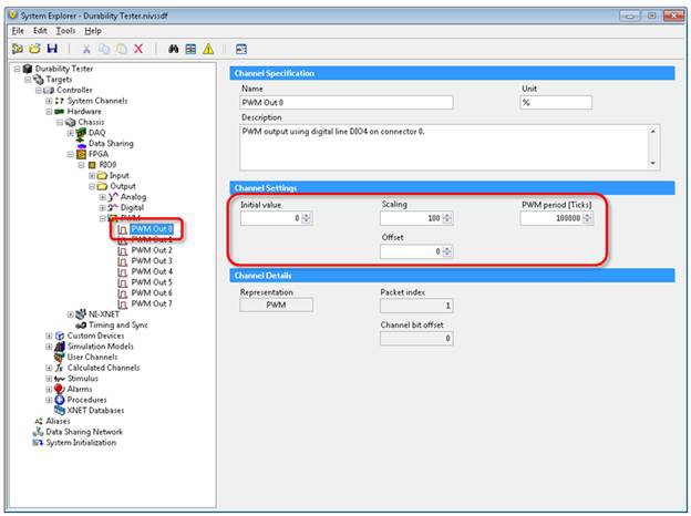
When creating NI VeriStand FPGA personalities, you start with a template project in NI LabVIEW software that includes the code necessary to interface to your NI VeriStand application. You use LabVIEW to define your custom FPGA functionality within this framework, compile the FPGA personality, and then edit the XML file for your FPGA personality. Once you have completed these steps, you can add this personality to an NI VeriStand system definition by simply selecting the XML file. The XML file tells NI VeriStand how to interface to your personality and automatically provide its inputs, outputs, and parameters inside the NI VeriStand System Explorer, so you can set your values and connections to other real-time tasks just as you would any other hardware interface. For example, if you have defined an FPGA personality with a PWM output, you can use the NI VeriStand System Explorer to set the channel parameters, such as period and initial value, and map the duty cycle input to another channel in your real-time testing application as shown in Figure 1.
Figure 1: Configuring NI VeriStand FPGA Personalities From the System Explorer
When you deploy your NI VeriStand real-time application, NI VeriStand automatically downloads your compiled FPGA personality to the hardware interface.
NI VeriStand FPGA Personality Architecture
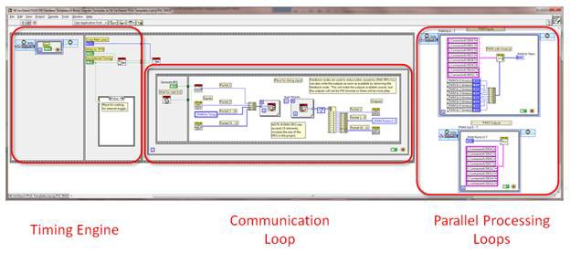
You create NI VeriStand FPGA personalities using the LabVIEW FPGA Module to modify the personality template that includes the code necessary to interface to your NI VeriStand application. FPGA personalities in NI VeriStand consist of a timing engine, communication loop, and parallel processing loops.
Figure 2: NI VeriStand FPGA Personality Template
Timing Engine
The timing engine, which is configured from the NI VeriStand System Explorer, synchronizes the FPGA to the NI VeriStand real-time application as well as other hardware I/O devices in the system. When your NI VeriStand real-time application is deployed, it loads your FPGA personality and the timing engine waits on a start condition from NI VeriStand.
Figure 3: Initializing Timing Engine
Before your real-time application asserts the Start trigger, NI VeriStand sets the parameters for Loop Rate (µs), Write to RTSI, and Use External Timing. These three parameters are responsible for configuring the timing engine’s synchronization mode (master, slave, or no synchronization) and setting the communication rate between your personality and the NI VeriStand real-time application.
The NI VeriStand – Generate PXI FPGA Clock subVI is responsible for generating the clock that times the communication loop discussed below as well as handling synchronization. In master mode, the FPGA times the communication loop with a loop timer running on the FPGA and exports a clock onto the Real-Time System Integration (RTSI) bus to synchronize the other hardware devices. In slave mode, the FPGA monitors the RTSI bus and times the communication loop with the clock captured on RTSI0. In No Synchronization mode, the FPGA times the communication loop with its loop timer and does not export anything onto the RTSI bus.
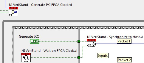
In addition to performing hardware synchronization, the timing engine allows for synchronization to the NI VeriStand real-time application. Part of the communication loop is shown in Figure 4.
Figure 4: NI VeriStand Synchronization to FPGA
The NI VeriStand – Wait on FPGA Clock subVI acts as the loop timer for the communication loop and waits for the clock from the NI VeriStand – Generate PXI FPGA Clock subVI. In master mode, NI VeriStand also asserts Generate IRQ prior to asserting the Start control. When Generate IRQ is asserted, the NI VeriStand – Synchronize to Host subVI asserts an interrupt on each iteration of the communication loop. If the FPGA is configured as the master, the NI VeriStand real-time application execution is timed by the FPGA via this IRQ signal.
Communication Loop
The communication loop is responsible for sending and receiving data to and from the NI VeriStand real-time application. Because NI VeriStand updates channels in a hardware-timed single-point fashion, the FPGA must run its communication loop at the rate specified by the Primary Control Loop in the NI VeriStand Engine. For more information about the NI VeriStand Engine, reference the NI VeriStand Help.
The communication loop is timed by the NI VeriStand – Wait on FPGA Clock subVI, which acts as a loop timer that waits on a clock generated by the NI VeriStand – Generate PXI FPGA Clock subVI discussed previously.
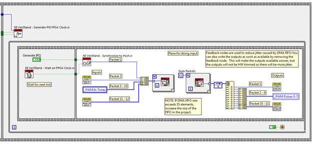
Figure 5: Data Communication Loop
As shown in Figure 5, data in the form of 64-bit packets is sent to the NI VeriStand real-time application via the DMA first-in-first-out memory buffer (FIFO) and data in the form of 64-bit packets is received from the NI VeriStand real-time application via the DMA FIFO.
The first packet sent to NI VeriStand contains information from the NI VeriStand – Synchronize to Host subVI that explains whether the FPGA loop is running late. The other packets sent to the host contain measurement or calculation data performed by the FPGA. The packets are sent by writing to the NI VeriStand – Send Packet to Host subVI inside a For Loop, which is responsible for writing to the DMA_READ FIFO. The DMA_READ FIFO is defined in the Project Explorer, and its depth must be specified to have at least as many elements as packets sent each iteration.
Data is sent to the FPGA via the DMA_WRITE FIFO, which is also defined in the Project Explorer. Its depth must also be specified to have at least as many elements as packets sent each iteration. The DMA_WRITE FIFO is read on the FPGA by the NI VeriStand – Receive Packet from Host subVI placed inside a For Loop. The For Loop must be configured to run the same number of iterations as packets that need to be read each iteration of the While Loop. The packets are then split up and sent to the appropriate parts of your FPGA personality. In Figure 5, the subVIs with yellow title bars signify I/O resources. Any I/O acquired and generated in this loop is synchronous to NI VeriStand and the other hardware devices in the system.
Parallel Processing Loops
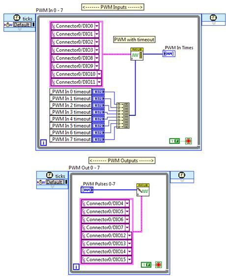
Parallel processing loops are the final part of a custom FPGA personality within the NI VeriStand framework. These loops are called parallel because they are not timed from the same clock that times the communication loop to NI VeriStand and the rest of the hardware in the system. These loops may simply be acquiring or generating data on I/O that has custom timing, or they may be responsible for custom measurements and generation such as PWM I/O. They may also be used for coprocessing data sent from NI VeriStand to the FPGA. The example template includes PWM inputs and outputs as shown in Figure 6.
Figure 6: Parallel PWM Loops
As seen in figures 5 and 6, the parallel processing loops send data to/from the communication loop via local variables. The communication loop updates these local variables only at the rate at which it runs, and it sends the current value of a local variable (no buffering) only to the NI VeriStand host. A parallel loop’s data is decimated by the communication loop, but the parallel loop’s timing is not affected by the communication loop.
Next Steps
FPGA-based I/O interfaces provide many advantages for real-time testing applications. They give you the ability to create custom I/O devices that can implement a combination of signal processing, simulation, triggering, and control tasks that can be easily reconfigured to adapt to new requirements or to create test systems capable of being used for multiple applications without changing hardware setups. NI VeriStand reduces the amount of development required to use FPGAs in real-time testing applications by providing a framework that implements the communication mechanism and data processing for you, so you can focus on the development of the FPGA functionality. You can then seamlessly plug the FPGA personality into NI VeriStand in the same manner as you would other hardware I/O interfaces and use the configuration-based environment to complete the rest of your real-time testing application.
