Anatomy of a Camera
Contents
- Solid State Cameras
- CCD Image Sensors
- CMOS Image Sensors
- Line-Scan Sensors
- Scanning Techniques
- Color Image Sensors
- Digital Cameras
Solid State Cameras
This document focuses on two types of solid-state cameras available today: CCD and Complementary Metal Oxide Semiconductor (CMOS). A solid-state camera is a camera that focuses incoming light onto a light-sensitive, solid-state (semiconductor) sensor. These sensors are typically made up of a rectangular array (imagers) or a single line (line-scan) of equi-spaced, discrete light-sensing elements, called photo-sites. Each photo-site acts as an optoelectric converter because it becomes electrically “charged” to a level directly proportional to the amount of light that strikes it during a given time period, called the integration time.
CCD Image Sensors
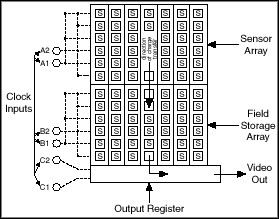
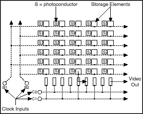
In a CCD design, the charges that build up on all of the array photo-sites are linked or “coupled” together so that they can be transferred out of the array directly (digital output) or processed into a time-varying video signal (analog output). Two basic designs have emerged during the past 20 to 30 years for transferring the accumulated charges out of a CCD array: frame-transfer (FT) and interline-transfer (IT), shown in Figures 1 and 2.

Frame Transfer CCDs
The simplest FT-CCD method employs a readout register and a CCD imager with its left side (active) exposed to light and its right side (storage) covered with an opaque material that makes these photo-sites insensitive to light. After the active photo-sites have been exposed for the integration time, the collected charges are transferred quickly into the storage area by applying an appropriate clocking sequence to the photo-sites of both areas. Then by properly synchronizing the storage area and the readout register, each line in the storage area is transferred sequentially into the output stage of the readout register. This allows the next frame of information to be collected in the active area while the current frame is being read out of the storage area. Optical shielding of the storage area and fast data transfer help to minimize image smear (the collection of spurious charges in the CCD’s photo-sites during transfer) in this design.

Interline Transfer CCDs
The IT-CCD design incorporates horizontally- or vertically-oriented, optically shielded readout strips of photo-sites located between the lines of active photo-sites in the array. This design operates in a similar fashion to the FT-CCD, except that much faster data transfer rates can be achieved due to the proximity of the active and readout sections of the array. This fact allows the entire image to be transferred simultaneously from the active photo-sites to the output stage of the readout register. However, because this design has shielded photo-sites that are also exposed to the incoming light distribution, the spatial resolution of the IT-CCD imager will typically be lower than that of a comparably sized FT-CCD imager.
CMOS Image Sensors
CMOS designs differ from CCD designs in the way the sensors are manufactured and how the charges are read out of the array. From a cost point of view, the biggest advantage that CMOS sensors have over CCD sensors is that CMOS sensors are manufactured on standard semiconductor production lines, whereas CCDs are manufactured on dedicated production lines. This advantage allows CMOS sensor designers to leverage the constantly improving manufacturing capabilities of standard CMOS production lines (larger wafers, smaller feature sizes) to incorporate onboard signal processing functionality at a fraction of the cost of CCDs. This manufacturing advantage allows CMOS sensors to be more tightly integrated into entire camera assemblies on a single production line than CCDs. However, CMOS sensors traditionally suffer from poor dynamic response when compared to CCDs. But with the rapid emergence of video-conferencing and high-performance, compact digital camera markets, a significant amount of research and development is being done to help remedy this and other deficiencies in CMOS designs. A definite design advantage that CMOS sensors have over CCDs is that each photo-site in a CMOS sensor array can have its own amplifier and output circuitry. This allows each photo-site to be read out independently of the other photo-sites and eliminates the need for charge-coupling. It also gives CMOS sensors the ability to have much better onboard programmability for more efficient read-outs and easier integration with “off-the-shelf” digital signal processors for more powerful and smaller overall camera design.
Line-Scan Sensors
Line-scan sensors can be manufactured from CCD or CMOS technologies as mentioned above; the only difference is that line-scan sensors are typically only one photo-site wide. This design feature makes line-scan sensors particularly well suited for production line inspection systems of rounded or cylindrical objects. The sensors are very simple and fast, and when used properly can be efficient for accurate inspection of these objects.
Scanning Techniques
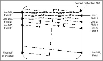
The scanning technique that a solid-state camera employs is usually dictated by the application. When television systems were first being developed about 50 years ago, it was made clear that many people’s vision systems had a measurable threshold on their ability to sense the movement of images over time, otherwise known as flicker. In an effort to minimize the unwanted effects of flicker, the television industry devised a method of interlacing or stitching two successive images read from a standard camera. The interlacing method they chose was quite simple and is still in use today on television and computer monitors worldwide. The technique, known as 2:1 interlace, is described by the following steps and shown in Figure 3:
- Read/display all even-numbered lines (even field, half-size)
- Restart
- Read/display all odd-numbered lines (odd field, half-size)
- Stitch the even and odd fields together and form a single, full-size frame
- Output the full-size frame

Figure 3: 2:1 Interlaced Scanning, Shown Here for the NTSC Video Format. PAL and SECAM Interlacing is Similar, with the Difference Being the Number of Lines in Each Field
With this established standard, solid-state camera manufacturers design this 2:1 interlace scanning technique into their cameras so that their cameras can be connected directly to standard televisions and monitors. Two simple variations on this technique are also implemented on some cameras: frame integration and field integration.
Frame Integration
In frame integration mode, only the even or odd field is repeatedly read from the image sensor, while the other field is discarded. This results in a full-size frame that contains only the even or odd field available on the image sensor.
Field Integration
In field integration mode, pairs of consecutive frame lines are read from the image sensor simultaneously, using all frame lines in the overall scan. For example, lines 1 and 2 would be combined and read as line 1, lines 2 and 3 would be combined as line 2, and so on, until a full-size frame is constructed.
From this description, it is clear that interlacing requires a finite amount of time to produce the final full-size frame. Furthermore, if any movement occurs in the scene between the time of the scans, the final frame will appear blurry. To combat these effects, new camera designs that employ progressive-scanning techniques have appeared on the market.
Progressive Scanning
Progressive-scan cameras operate by immediately transferring an entire frame at once from the image sensor without any performing any line-interlacing. The obvious benefit of this design is in motion detection applications, but the down side is incompatibility with standard television systems. However, computer-based image processing applications do not require that raw camera images be displayed on a television monitor. Rather, the camera is used as the sensor and input device to a plug-in acquisition board inside a computer with a built-in display board that can handle the output of the acquisition board directly. Progressive-scan camera designs are gaining in popularity for these computer-based applications, because they incorporate direct digital output and eliminate many other time-consuming and unnecessary processing steps associated with television systems.
Color Image Sensors
Up to now, the discussion has been focused on the how solid-state imagers produce a representation of the intensity field present in an image only. But intensity or brightness is only one attribute associated with how we perceive the sensation of “color.” Two other attributes complete the picture: hue and saturation. The hue of an object represents the wavelength of light that our vision system sees when it is focused on the object. Hue is commonly referred to the object’s color; that is, red, orange or green, etc. Saturation represents the amount of gray light contained in the color relative to its hue. Saturation is commonly referred to the color’s strength or purity.
Unfortunately, image sensors that can detect hue, saturation, and intensity directly do not exist. But in 1960, physiologists found that the peak light absorption characteristics of the three types of cones (color sensing components) in the human eye nearly correspond to the red, green, and blue wavelength regions of the visible light spectrum. So, it is no coincidence that when you mix red, green, and blue primary colors in the proportions, you can produce millions of new colors. This “tristimulus” color model can be seen in nearly every device used with colors (computer monitors and printers, for example). Because the output signal of a CCD or CMOS image sensor is proportional to the incident light intensity, you can make a simple color image sensor using tristimulus color theory. In practice, this has been done either by using three image sensors, each having its own spectral response characteristics (the three-chip design), or by using a single sensor and a color filter array (the single-chip design).

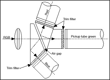
Figure 4: Three-CCD Beam Splitter Optics
Three-Chip Sensors
In a typical three-chip design, light that enters the camera housing is first split into three beams and then focused onto three CCD arrays, each of which has a color filter laminated to the light sensitive side of the array. This method has been very popular, because the spectral response function characteristics of the color filters can be designed to simulate those of the human eye, thus enabling the camera to behave like the color vision model presented earlier. The benefits of this design include simple signal processing, very accurate color reproduction and control, and high resolution. However, cameras that employ this design tend to be expensive and large in size, because of the added electronics associated with the three sensors. But more importantly, they typically suffer from poor low-light sensitivity due to the lower signal levels obtained from beam splitting.
Single-Chip Color Sensors
In a typical single-chip design, a carefully selected color filter array (CFA), is laminated directly to the light-sensitive side of a CCD image sensor. More complicated electronics and interpolation algorithms are required in this design, but these cameras are typically much smaller, less expensive, and have better low-light sensitivity than three-chip designs. The main drawbacks of the single-chip design are lower resolution and less accurate color reproduction and control.
Color Filtering Techniques
The CFA is typically constructed as a repeating sequence of three colors (that is, red, green, and blue), each having its own spectral response functions. The sequences are arranged to form either a horizontal or vertical stripe pattern or a checkerboard pattern. Stripe filter patterns typically require less complicated signal processing electronics than those having checkerboard patterns and they will produce images with superior horizontal or vertical sharpness (Parulski, 1985). However, some checkerboard patterns can give better overall performance by taking advantage of the added geometric flexibility inherent in checkerboard patterns (Bayer, 1976).
Digital Cameras
Digital cameras have several technical advantages over analog cameras. By digitizing at the CCD camera rather than at the image acquisition board, the signal-to-noise ratio is typically higher, which results in better image resolution. Many digital cameras now come with 8- to 12-bit gray levels of resolution as a standard feature. This higher image resolution is often required in medical, machine vision, astronomy, and thermal imaging applications. The National Instruments IMAQ 142x series are digital image acquisition boards designed to work with digital cameras from many manufacturers. Digital cameras typically have one or more 8-, 10-, or 12-bit channels (often called taps). These channels are the streams of digitized data from the CCD sensor array. These channels can be read out in parallel from the camera for fast digital image acquisition. Some digital cameras can output data at a rate greater than 100 Mbytes/s. The IMAQ 142x series boards have a 40 MHz pixel clock and can acquire at a rate of 160 Mbytes/s or more. In addition, you should consider having a memory buffer on your digital frame grabber. With an onboard memory buffer, you can acquire at extremely high rates while sustaining high-speed throughput and greater overall system performance.