Next-Generation Semiconductor Technology Parametric Test
Bart De Wachter, imec Semiconductor Technology and Systems Group Researcher
Case Study Highlights
- Reducing wafer loss and costs by implementing in-line electrical test, measurement, and analysis
Reducing fab cycle time by 3X using 24 dedicated parallel SMU channels (one per probe needle) in a small form factor
Further improving system capabilities by implementing flexible test and measurement routines using LabVIEW
"The test-time reduction using this SMU-per-pin method is nothing short of spectacular, and wouldn’t be possible with large, traditional box SMUs. Our method eliminated switching and serialized-measurement time, reducing total test time to that of testing a single test point."
—Bart De Wachter, imec Semiconductor Technology and Systems Group Researcher
The Challenge:
Performing accurate electrical wafer-level tests in the semiconductor R&D fabrication (fab) process flow to detect process-related issues at an early stage. This helps us rework the wafers at the right time to manage yield drops and optimize the R&D process flow, reduce costs, and decrease the time-to-market of the newest chip-manufacturing techniques.
The Solution:
Using the NI PXI platform with PXIe-4135 source measure units (SMUs) to build a highly parallel measurement system to use inside the wafer fab, and programming this setup with LabVIEW so that we can keep all of the wafers inside and test them, process the results, and make much faster adjustments to the semiconductor process flow.
Introduction
Imec is a leading independent European nanotechnology research center. We bring together key players from all layers of the semiconductor industry—from tool and material suppliers, to integrated device manufactures and foundries, to fabless and fab-lite companies, to application partners.
Thanks to our close partnerships with leading tool and materials suppliers, we can perform advanced semiconductor process development and offer our partners the industry’s most advanced research infrastructure housed within a state-of-the-art 300 mm wafer fab/clean room.
Our diverse, advanced semiconductor technology and processing R&D includes next-generation logic devices, advanced nanointerconnect research, and heterogeneous 3D stacked integrated control (IC) system integration, paving the way for future low-power mobile applications.
Fab Process Flow Challenges
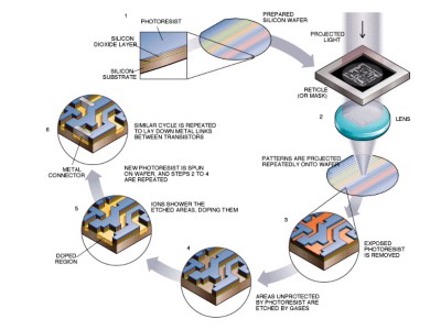
We perform wafer/chip processing by sequentially running through hundreds of dedicated process steps (called process flow), starting from a blank silicon wafer and ending with an electrical functional chip. However, given the nature of the R&D environment and the complexity of individual process steps, defects that occur over the length of the entire process flow result in a significant functional-device yield drop.
Electrically testing individual chips/devices on wafers early in the process flow provides on-chip device performance feedback and early semiconductor process monitoring. However, because our previous setup did not have an in-line electrical test setup embedded in the fab, we could not obtain feedback at critical points in the process flow. We were forced to take wafers out of the fab to test them on the existing parametric testers at an incomplete stage in the process. And because wafers that went out of fab could not return for further processing due to contamination issues, we experienced significant wafer losses and a big delay in the learning cycle and project deliverables.![]()
Our R&D test chip vehicles consist of thousands of individual transistors, resistors, and capacitors with a wide variety of dimensions and architectures. They also may include small demonstrator circuits. We need to test all these devices to correctly characterize a specific semiconductor manufacturing process.
An in-fab semiconductor automated test equipment (ATE) setup capable of handling 24/7 test operations could significantly reduce R&D project deliverable time and decrease overall cost. We didn’t have a valid electrical test solution in our wafer fab, so we started looking for a versatile setup that could perform tests quickly and accurately to support our various industry affiliation programs. The setup needed to cover all of our parametric and functional IC test needs and easily expand for future semiconductor process technology tests.
Phase 1: Implementing an In-Fab, High-Throughput, Highly Accurate ATE Setup
In the past, we performed these tests on traditional parametric testers outside of the fab. While they worked sufficiently, we had to produce twice the number of wafers because the tests were performed outside of the fab: One set stayed in the fab and the other was tested outside of the fab. This time-consuming approach meant that we had to take the lessons learned from the tested batch and apply them to the wafers currently in the fab during the rest of the processing steps.
To reduce this overhead, we began looking for alternative solutions. We required a supplier that would deliver superb hardware and software service support. Quickly, we noticed that testers on the market either focus on parametric test or functional test, but not both. Also, traditional parametric testers utilize switch matrices to share SMU, digital multimeter (DMM), and LCR meter resources, which can degrade signal integrity and inherently serializes operations. Additionally, they usually take a long time to program, come in a fixed package, and are expensive.
We chose the NI PXI platform for general test, validation, and measurement activities, and enjoy an outstanding relationship with NI. We knew NI could deliver the hardware and software service support we needed. Once we realized that NI was working on a next-generation, highly accurate SMU, we saw an opening to build a cost-efficient system and improve our in-fab measurement capabilities. Having insight into NI’s roadmap led to us engaging with them as an early adopter of new technology.
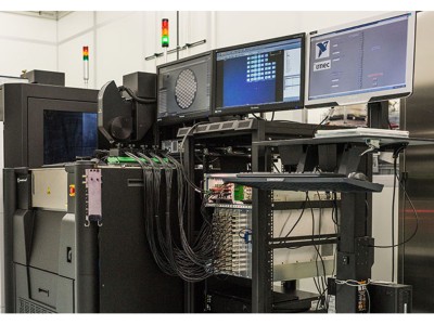
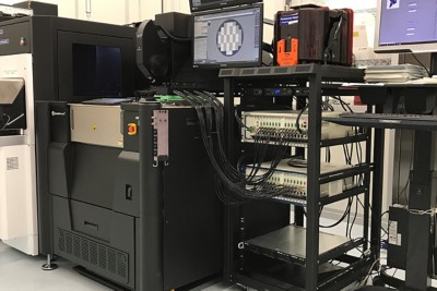
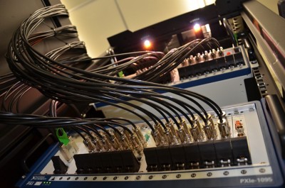
We used the PXIe-4135 femtoampere-class SMU and the PXI platform to build an in-fab ATE system that can run 24/7, drastically decreasing our project timelines and helping us avoid wafer waste. In addition to the PXI instrumentation, we used a probe station equipped with an automatic wafer-handling system that could run unattended. We developed a custom probe card and hooked up all wafer-probing components to a 19 in. rack housing the PXI instrumentation.
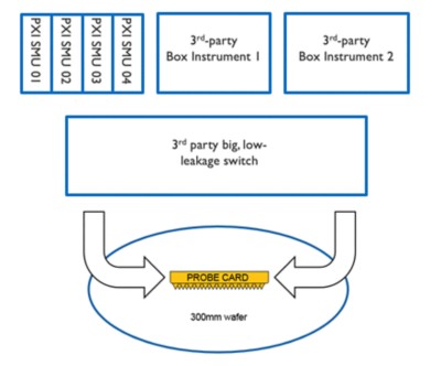
Our initial tester version combined NI PXI SMUs with a DMM, LCR meter, and third-party low-leakage switch matrix to share resources across test points. The PXIe-4135 triaxial cables were critical to preserve low leakage levels throughout the entire setup.
Programming the Setup with LabVIEW and Obtaining Initial Results
We developed, implemented, and benchmarked a library of LabVIEW parametric test routines on the in-fab ATE using PXI modular instruments for measurements on process monitor structures. We implemented customized LabVIEW test sequences for fully automated, unattended wafer test at several stages of the process flow. These sequences control and synchronize the NI instrumentation, switch, probe station, and autoloader. Using LabVIEW, we logged all data in an imec data-warehouse-compatible format to smoothly overlay electrical data with other inline (optical) metrology data and provide in-depth process analysis.
A typical SMU-to-transistor hookup scheme consists of applying the four PXIe-4135 SMUs to the gate, drain, bulk, and source terminals (Figure 7) and using individual force and sense connections through the switch matrix to rule out parasitic components. We submitted a complete LabVIEW transistor test suite on wafer—including on-state/off-state current measurements, sweep measurements, and threshold voltage extraction procedures—and benchmarked the results with high-end third-party instrumentation.
Figure 8 demonstrates that the PXIe-4135 SMUs are equivalent to high-end third-party instrumentation for I-V, and even C-V, measurements.
PXI Platform Impact on Fab Activities
With the in-fab ATE, we can perform experiments that were previously impossible or came at a high-wafer-count cost. These new experiments provide valuable insight that we, as an independent research organization, need in order to develop next-generation semiconductor industry process technologies.
Figure 9 shows impressive improvements for one of these experiments:
Phase 2: Improving Parallelism and Test Execution Time
At this point, we had already demonstrated that the PXIe-4135 is on par with the highest quality SMUs on the market for I-V test and, due to the high-speed sampling rate capabilities, it is even suited to do low-frequency, picofarad-level C-V tests, as well. Due to the versatility of this SMU, we can get rid of the DMM and LCR meter and stick to one type of instrument for all required PCM testing.
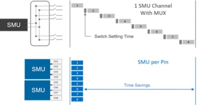
Using the PXIe-4135 as our only instrument reduced test costs, but we also had ambitions of further improving test time. The PXIe-4135 SMU’s small form factor and superior performance meant that we could ditch the bulky switch matrix and use an SMU-per-pin architecture to connect individual high-performance SMUs directly to each of the various test points within a probe pad module, reduce the signal path, and test them all in parallel.
The newest in-fab ATE system hardware configuration now consists of two daisy-chained PXI chassis, 25 PXIe-4135 SMUs (24 connected to probes for top-contacting the wafer and one for chuck contact), and one powerful RMC-8356 rack-mount controller. The prober and wafer-loader are controlled through a GPIB-USB interface, and we kept LabVIEW at the heart of the software architecture.
The test-time reduction using this SMU-per-pin method is nothing short of spectacular, and wouldn’t be possible with large, traditional box SMUs. Our method eliminated switching and serialized-measurement time, reducing total test time to that of testing a single test point.
For example, imagine a probe pad module with 24 pads and 12 diodes; each diode connected to two pads. For diode leakage measurements in the femtoampere range, we need to use long test integration (aperture) times to reject measurement noise. These integration times can be as long as 32 power line cycles (PLC), which equates to 640 ms (32 PLC x 20 ms/PLC). In a conservative sequential test setup with a switch matrix, the switching and settling times, which typically run roughly 10 ms, also are a factor. Taking that into account, our Phase 1 setup would require roughly 7.92 s per probe pad module. For the highly parallel setup, we effectively reduced the test time to the measurement time of one diode (640 ms), or 12X faster.
After acquiring test-time data across a number of applications and factoring in prober-stepping time, we are 3.35X faster, going from 67 minutes per wafer on a traditional setup down to 20 minutes per wafer on the highly parallel setup. So, we can safely say that our test throughput has tripled from Phase 1 to Phase 2! The throughput increase helps us release our R&D project deliverables significantly quicker, as the process-learning cycles are becoming much shorter. Furthermore, we can extract big datasets for wafer-level reliability studies early in the process flow.
Organizational and Business Impact
Our ATE setup has become an indispensable tool for monitoring Imec’s leading-edge semiconductor processes. All wafers coming over for electrical test can resume processing afterwards. There’s no need to take the wafers out of the fab anymore. This saves dozens of wafers a year for each of our industry affiliation programs. The learning cycle has become significantly shorter as well, which means that we can finish projects sooner and perform more research in the same amount of time.
Whenever the embedded electrical test, followed by fast data analysis, proves that process conditions are out of spec and need to be tweaked, we can pull wafers back one or more steps in the process flow for a complete rework with updated process conditions. We can test again and continue processing or iterate the rework/test cycle time and time again. We have significantly reduced the wafer loss caused by experimental/bad processing.
One of our process integration engineers said, “In-line electrical test has become the only way to prove that we obtain valid process conditions. We cannot wait with test until the wafers have finalized processing, as it would lead up to one month of delay in the learning cycle. In-line electrical measurements can capture many process-related issues originating from patterning, metallization, and planarization steps at an early stage in the wafer manufacturing process.”
Conclusion and Next Steps
The PXIe-4135 has proven to be a highly accurate SMU and can double as a C-V measurement unit, saving costly instrument and test channel expansion. Demand for in-line testing has grown significantly over the last few months and continues to do so. Increasing the test throughput and reducing the overall test time are among our challenges. Wafer fab cycle time is extremely important. To tackle these challenges, we plan to improve and extend our LabVIEW parametric test procedure library and potentially evaluate TestStand software for a higher level of automation, operator friendly usage, and easy data handling.

