Interconnect Considerations for MIPI® RFFE℠
Overview
The MIPI RF Front-End Control Interface (RFFE) specification operates within this range, and you may find scaling the requirements from the application environment (mobile devices) to a test setup challenging. However, with recommended design practices, you can use NI PXI Digital Pattern Instruments to reliably communicate via MIPI RFFE with DUTs at clock frequencies up to 52 MHz through interconnects up to 2 m. This paper shows how to design, set up, and debug systems using high-speed digital buses and examines the theory behind these recommendations.
Note that while this document focuses on MIPI RFFE, several of the concepts generally apply to many high-speed digital buses.
Contents
Design Recommendations
You need to follow a few basic rules when building a high-speed digital test system and when probing/debugging these systems:
- Design all interconnects between the Digital Pattern Instrument and the DUT with 50 Ω characteristic impedance. This includes all components in the signal path such as sockets, load boards, cables, connectors, and adapters.
- Use time-domain reflectometry (TDR) to measure and compensate for the propagation delay of the interconnect. To use TDR effectively, you must be able to remove the DUT from the end of the signal path or put it into a high-impedance mode.
- Add more cycles to a pattern if you need to prevent collisions between the DUT taking over the bus and the previous, delayed signal of the DUT parking the bus.
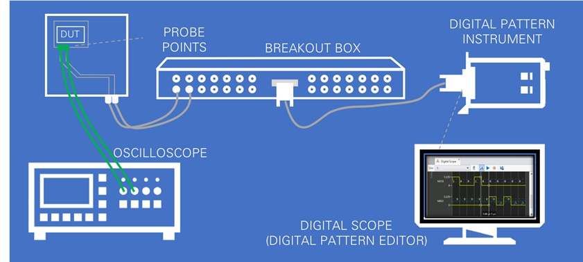
- When probing with an oscilloscope, probe as close as possible to the point at which you must receive a signal. This point is close to either the DUT or the Digital Pattern Instrument, depending on the operation. When you receive the signal of the Digital Pattern Instrument, use the Digital Scope feature in the Digital Pattern Editor to probe the signal. When probing signals received by the DUT, use a separate oscilloscope at probe points on the load board near the DUT.
- When viewing signal waveforms, evaluate the receiving side only when it is receiving for the best representation of the signal.
Designing With 50 Ω Interconnect Impedance
The Digital Pattern Instrument has a 50 Ω impedance. To achieve the best signal quality, ensure that all interconnects between the instrument and the DUT have a characteristic impedance of 50 Ω. This includes all components in the signal path such as sockets, load boards, cables, connectors, and adapters.
Figure 1. Every component along the signal path should be designed with a 50 Ω impedance if possible.
NI VHDCI cables and the NI SMB-2163 breakout box have a characteristic impedance of 50 Ω. You can easily purchase 50 Ω coaxial cables with SMB connectors on one end and various connectors on the other end such as SMB, SMA, or BNC.
When designing a load board, you should design traces to 50 Ω. For an STS DX system, use the recommended spring pin landing pad layout. For STS CX or a stand-alone PXI chassis, use a VHDCI cable with the VHDCI connector on the front panel of the instrument. Coaxial connectors to coaxial cables to an SMB-2163 Terminal Block are also acceptable and allow for extended temperature operation.
When designing a load board with a VHDCI connector, ensure that each of the bus pins on that connector is next to another pin connected directly to a ground plane. Each signal pin should have a separate dedicated ground pin.
Every manufactured item has tolerances listed in its specifications. Most cables and PCBs have impedance tolerances around ±10 percent, which is suitable for MIPI RFFE.
Any new system should be designed to be 50 Ω. If the load boards and connectors in an existing system are not exactly 50 Ω, these systems may still communicate reliably at high speeds. For these systems, perform characterization to determine voltage and timing margins.
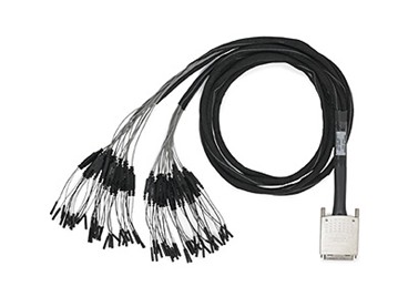
For example, the NI SHC68-H1X38 flying-lead cable is not perfectly controlled to 50 Ω and does not maintain controlled impedance through the flying-lead portion. Reflections from this impedance discontinuity cause signal distortion that is noticeable on a scope, but many DUTs can run reliably at 52 MHz or higher in spite of the reduced signal quality.
Figure 2. The SHC68-H1X38 Digital Cable breaks out the VHDCI pins to individual flying leads, which are not impedance-controlled to 50 Ω.
When driving a signal, the DUT itself has an output impedance that may not be exactly 50 Ω. This can limit performance for longer interconnect lengths. Output impedance is another way of describing drive strength. Higher drive strength correlates with lower output impedance and vice versa. If the DUT has programmable drive strength, adjusting that drive strength (output impedance) may improve your results. See the section on DUT output impedance mismatch for more details.
Using Time-Domain Reflectometry (TDR)
With a 2 m cable at 52 MHz, the propagation delay of the cable is long enough that by the time a signal propagates from the instrument to the DUT and back, the instrument is already starting the next cycle. This can be confusing when calculating strobes and delays and when using the Digital Scope feature for debugging.
You can perform time-domain reflectometry (TDR) measurements interactively through the NI-Digital Pattern Driver and Digital Pattern Editor or programmatically through the API. TDR is used to measure the time delay for each channel from the instrument’s timing calibration plane to the DUT socket. Drive and compare times are then automatically adjusted to account for these delays, which removes the need for you to design these delays into your timing settings. Note that the timing calibration plan is the POGO interface for an STS DX system; otherwise, it’s the front panel of the Digital Pattern Instrument.
To make a TDR measurement, you must have a 50 Ω interconnect with an open circuit (or high impedance) at the far end. You need to remove any substantial capacitive or resistive loads on the load board to take TDR measurements.
When you use the Digital Pattern Editor, your TDR values are not stored. You need to either rerun TDR measurements each time you open the Digital Pattern Editor or store the values and reapply them each time. You can copy the TDR values from the Digital Pattern Editor to a spreadsheet or text file and then paste them back in when you rerun the Digital Pattern Editor.
You should use TDR to align your timing, but you may need to take more action. TDR delay values do not help in the case of a bidirectional data line, where one end drives and then parks the bus, and then the other end drives. You face the potential for collision if the round-trip propagation is as long as the cycle time. You can “stretch” bus park cycles to handle these cases.
“Stretching” Bus Park Cycles
The bidirectional data line in MIPI RFFE requires a bus park cycle when data switches direction. The hardware parking the bus drives the data line low during the first half of the cycle and releases the data line during the second half of the cycle. The hardware taking over the bus can then start driving in the second half of the cycle and drive its data bits on subsequent cycles.
But, if the interconnect’s propagation delay is long enough compared with the cycle time, the hardware that is taking over the bus can start driving while the last bit driven by the hardware giving up the bus is still propagating down the interconnect. The last data bit will be double driven and possibly corrupted.
This problem usually occurs when the instrument is reading a register on the DUT. The instrument drives the clock to the DUT and in response to the clock edge while the DUT drives its last data bit (parity). On the next cycle, the DUT parks the bus by driving during the first half cycle, and the instrument takes over by driving on the second half cycle. But the instrument starts driving before the clock can get to the DUT and the DUT can send the parity bit back in response. Thus, the instrument drives against the parity bit, which leads to an intermediate voltage value.
Figure 3. An intermediate voltage is caused by the instrument driving against the parity bit from the DUT.
To fix this, you can use an additional delay when the instrument first drives, either through a special time set or by padding additional cycles into the pattern. Your specific propagation delays, cable length, and clock period determine which, if any, of these extra cycles you need.
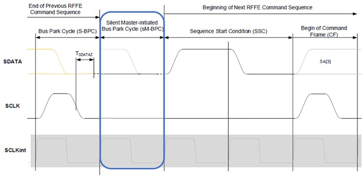
Figure 4. By stretching the bus park cycle, you give the instrument more time to receive the parity bit. Note that this is not the same as the Silent Master-initiated Bus Park Cycle (sM-BPC) described in MIPI RFFE v2.1. The sM-BPC adds an extra period during which the master drives the data signal in case the slave stops driving too soon to drive the data line all the way low. Unlike with the sM-BPC, when stretching the bus park cycle the master does not drive the data signal. The above image was used with permission from MIPI Alliance, Inc.
Using Effective Probing Points
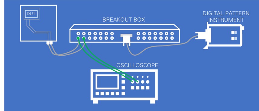
Because of signal reflections, observed waveforms almost always look worse near the center of the interconnect. For the most accurate representation of the signal received by the hardware, probe as close to the receiving end as possible—within 2 to 3 inches should be good enough.
Figure 5. Probing at the center of the signal path does not show what the receiving end sees, which could lead to inaccurate conclusions about the signal.
Figure 6. Probing much closer to the DUT generates a much more accurate representation of the signal received by the DUT. The clock signal generated by the instrument looks much nicer. For signals received by the instrument, use the Digital Scope feature of the Digital Pattern Editor.
Evaluating Waveforms: Where and When
Even if you probe right at the hardware itself, signals often look bad from the perspective of the driving hardware because of reflections. This is how a digital signal line is expected to work; the waveform at the receiving end is what matters. For the bidirectional MIPI RFFE data line, keep in mind when hardware is driving and when it’s receiving.
Look at a simple register read:
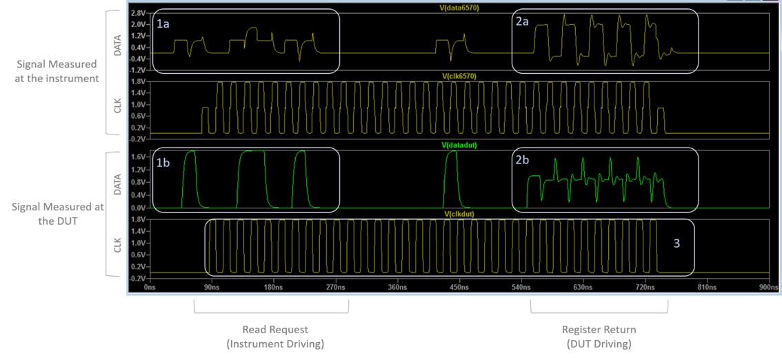
Figure 7. If you measure the signal at the driving end, the signal will look much more distorted. It’s recommended to observe the signal at the receiving end.
During the read request, the instrument is driving the data line with the command and address bits while the DUT is on the receiving end. The signal measured at the instrument (1a) looks very distorted; however, the signal measured at the DUT (1b) looks great. This is the signal you should watch during this time.
During the register return sequence, the DUT is driving the data line with the register data while the instrument is on the receiving end. Again, the signal on the transmitting side (2b) looks much worse than the signal on the receiving side (2a).
Also notice that because the instrument is always driving the clock, you should evaluate the signal at the DUT (3).
Theory
Much of the confusion when running digital buses at higher speeds through longer cables originates from the effects of transmission line theory. As voltages switch faster and more frequently, you can no longer treat a wire as a single point with the same voltage throughout, but instead you need to take into account the transitions taking place over time.
The first significant effect of transmission line theory is propagation delay. A voltage change takes a nontrivial amount of time to propagate from one end of a cable to another. Thus, one end of the cable may be at a different voltage than the other end.
The second significant effect is characteristic impedance. Any cable or other interconnect has a property known as characteristic impedance. Although the cable’s DC resistance may be only an ohm or so under steady-state (DC) conditions, during that propagation delay time, while a voltage change is working its way from one end of the cable to the other, the cable has a different impedance, typically 50 Ω for NI’s VHDCI cables. This transient impedance is called the characteristic impedance, and it determines the voltage-to-current relationship during the propagation delay time.
The third significant effect is reflection. When the impedance of the instrument or DUT at the end of the cable does not match the characteristic impedance of the cable, voltage transitions reflect backward off that end and propagate back down the cable to the source of the transition.
These three effects can produce strange-looking waveforms at some places and times. If you set up your system correctly, the strange-looking waveforms appear at places and times you don’t care about, and you have better-looking waveforms at the places and times you do care about. And, with some understanding of transmission line theory, you know when and where to care and not to care.
Illustration: Propagation Delay
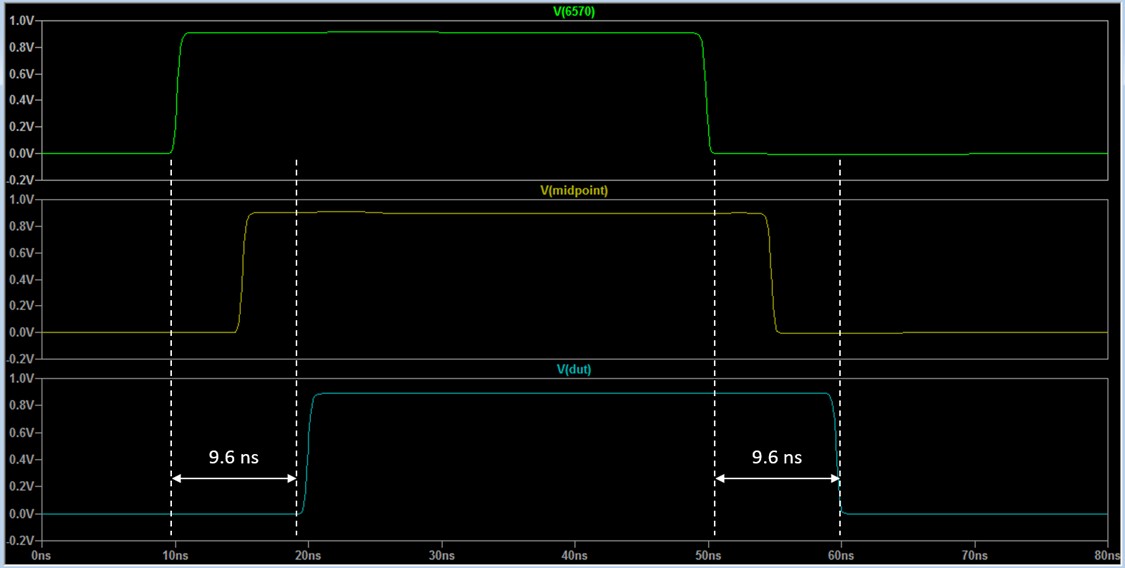
The simulation in Figure 8 demonstrates the propagation delay across a 2 m VHDCI cable. The model consists of a simulated PXIe-6570 digital pattern instrument, a 2 m VHDCI cable (broken up into two 1 m sections to measure at the midpoint), and a DUT with a simple 50 Ω load.
Note that this is an uncommon impedance value for a DUT. DUTs typically have high impedance values (50 kΩ or more). You are matching the impedance in this example to avoid signal reflections, which this paper addresses later.
Figure 8. This model simulates a PXIe-6570 driving a signal into a 50 Ω DUT.
The voltage rises at the driver/instrument (green waveform) immediately. It changes at the DUT (blue waveform) only after a delay of 9.6 ns. The yellow waveform at the midpoint of the cable shows the transition at half the time.
Figure 9. Notice the delay in signal changes between the instrument, the midpoint, and receiving DUT.
You can see the same delay from the time the instrument drives the signal low until the time the voltage at the DUT becomes low. This confirms the propagation delay specification for the 2 m NI SHC68-C68-D4 Cable:
Figure 10. The documentation for the SHC68-C68-D4 Cable specifies the propagation delay for various lengths.
Illustration: Characteristic Impedance
To learn more about characteristic impedance, explore the same model except the DUT has a resistance of 1 Ω to match the resistance of the 2 m VHDCI cable. Notice the difference between the resistance and the characteristic impedance of the cable.
Note that this is an uncommon impedance value for a DUT. DUTs typically have high impedance values (50 kΩ or more). This example uses a 1 Ω resistance to simplify the illustration.
Figure 11. This model (top) simulates a PXIe-6570 driving a signal into a 1 Ω DUT. The documentation for the SHC68-C68-D4 Cable specifies the characteristic impedance and resistance for each length. Notice that the characteristic impedance does not change with the length.
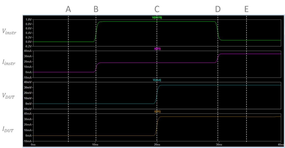
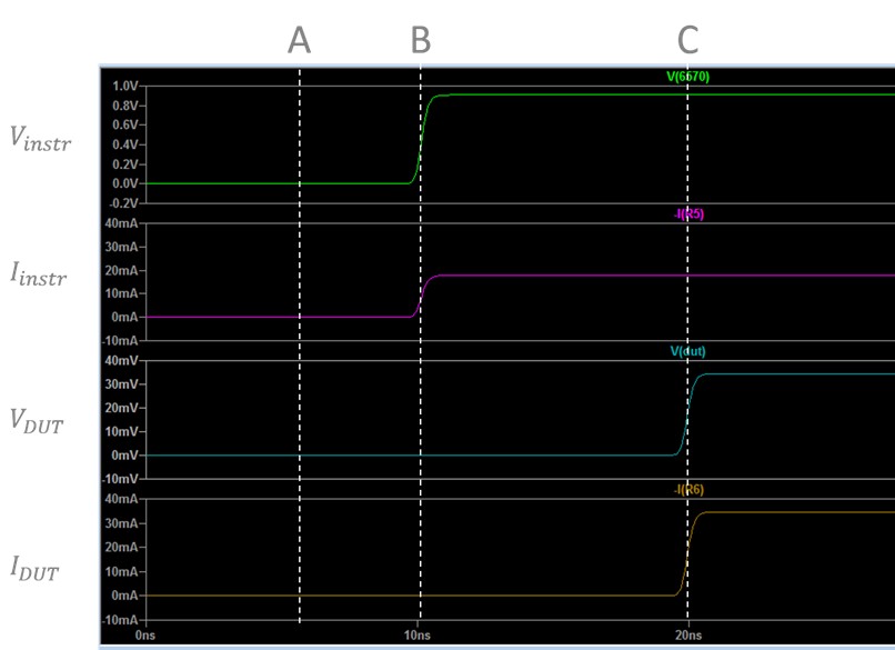
In Figure 12, the voltage and current at both the instrument and DUT are shown for the instrument transitioning from driving 0 V to driving 1.8 V. See the descriptions of each marked point below to understand how characteristic impedance, resistance, and propagation delay contribute to the waveforms displayed.
Figure 12. Note that the instrument voltage (Vinstr) and the DUT voltage (VDUT) use different scales.
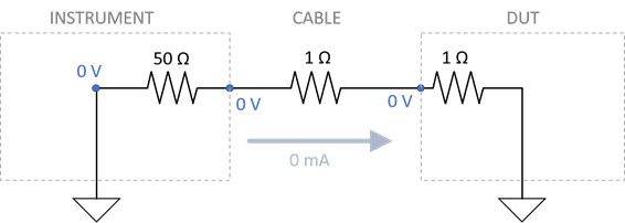
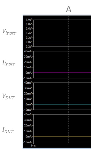
A. In steady state, while the instrument (left) is driving the voltage to 0 V, every point in the circuit is at 0 V and there is no current flow.
Figure 13. At point A, the instrument is driving 0 V into ground, so the current has no voltage or current (steady state).
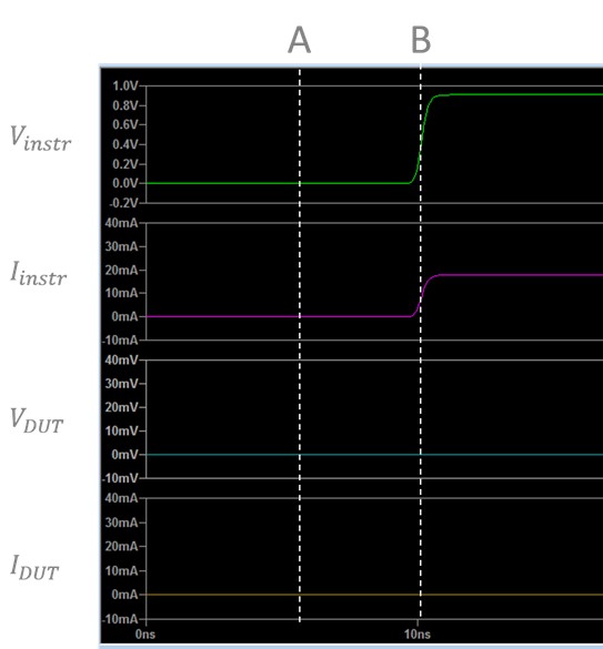
B. When the instrument begins driving 1.8 V, the circuit enters a transient state due to the propagation delay in the system. The instrument is “unaware” of the DUT at the other end of the cable, and the voltage and current experienced by the instrument are functions of the characteristic impedance, or the impedance associated with the distributed capacitance in the cable. At the same time, the DUT on the other side of the circuit is not aware of any changes in the circuit and operates under the assumption that the other end of the circuit is still generating 0 V.
Figure 14. During the transient state after point B, the instrument and DUT behave under different assumptions. The instrument acts as if a voltage divider is created between its own impedance and the characteristic impedance of the cable (left circuit). The DUT continues to operate as if the DUT (right circuit) is driving the 0 V.
C. After a delay of 9.6 ns, the signal reaches the end of the cable and the DUT “sees” the instrument and cable in the system. It now operates like a simple DC voltage divider and replaces the characteristic impedance of the cable with the actual impedance of the instrument and the resistance of the cable. The instrument is still unaware of the changes the DUT caused, so it continues to operate under the previous assumptions until it receives a signal reflection.
Figure 15. At point C, the signal has reached the DUT and raised the voltage at the DUT to its final value, which is now based on the actual resistance of the cable and the instrument impedance. After point C, the signal’s reflection heads back toward the instrument.
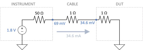
D. After another delay of 9.6 ns, the signal reflection reaches the instrument and “sees” the full circuit. It now also operates like a simple DC voltage divider. Both instruments now operate under the same assumptions with the instrument measuring 69 mV and the DUT measuring 34.6 mV. This is the new steady state until another change occurs in the driven signal.
Figure 16. At point D, the reflection reaches the instrument and lowers the voltage at the instrument. The voltage drop across the instrument is now based on the nontransient impedance values of the circuit. A new steady state continues through point E.
Illustration: Reflections
High-Impedance Receiver
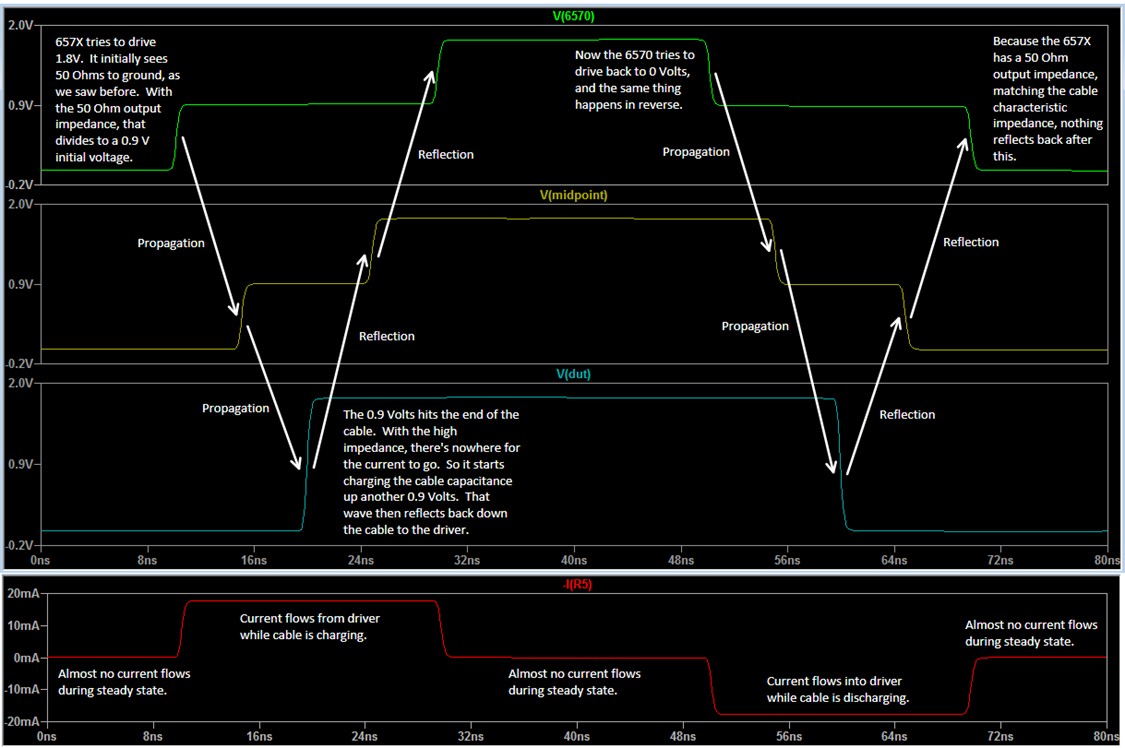
The characteristic impedance illustration showed where the voltage waveform reflected off a low impedance back to the driver. Here you see a high impedance at the receiver, which is typical of most DUTs when they are receiving. This causes a positive voltage reflection from the receiver.
The waveform at the driver and the midpoint has voltage “shelves,” where the voltage temporarily switches only halfway until the reflection comes back and drives the voltage all the way up or down. The voltage at the receiver, however, has nice, clean, full voltage edges, and the receiver is where you care how the waveform looks.
This is called “reflected wave switching,” with a 50 Ω driver and a high impedance receiver, and is the way many digital systems are designed to work.
Figure 17. This model (top) simulates a PXIe-6570 driving a signal into a high-impedance (50 KΩ) DUT. The PXIe-6570 experiences “jumps” in the measured voltage due to the reflection’s propagation through the line.
Changing Frequency
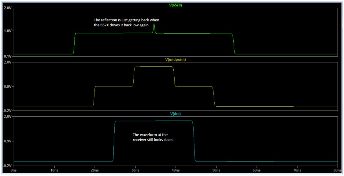
If you increase the clock frequency (decrease the pulse width) to where the pulse width is almost equal to the round-trip of propagation and reflection, then the voltage at the driver never quite gets to its final value. Notice how the receiver waveform still looks good in Figure 18.
Figure 18. As signal frequencies become higher, the full-voltage “plateau” measured by the driving instrument becomes smaller.
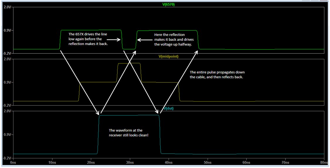
If you decrease the pulse width still further, the reflection doesn’t have time to get back before the instrument drives the line low again. Later, the reflection does get back and drives against the instrument, which creates a second half height pulse. Again, notice how the receiver waveform still looks good. This seems counterintuitive; you see two half height pulses at the driver and one full height pulse at the receiver! But that’s what actually happens, and that’s why you shouldn’t worry about what the waveform looks like at the driver. It can bear little resemblance to the waveform at the receiver.
Figure 19. Sometimes the driver will never experience full voltage due to the high frequency of the signal. This doesn’t matter because it is the voltage at the receiving end that we care about.
DUT Output Impedance Mismatch
If the DUT has an output impedance equal to 50 Ω, it produces a clean waveform at the PXIe-6570 digital pattern instrument, just like that shown in Figure 19 for the PXIe-6570 driving the DUT. If the DUT’s output impedance is not 50 Ω, you see stairsteps at the receiving (PXIe-6570) end of the cable like the ones shown in Figure 19 for the midpoint of the cable.
Consider the simulation in Figure 20 of a DUT with 100 Ω output impedance instead of 50 Ω. Note that output impedance is just another way of specifying drive strength. Higher drive strength means lower output impedance and vice versa. For DUTs with programmable drive strength, you should adjust the drive strength to the setting that produces the cleanest edges on the PXIe-6570 digital scope.
If the DUT does not have programmable drive strength, then you cannot improve the edges and you may need some workarounds to achieve your desired performance. The following example simulates a DUT with 100 Ω output impedance (drive strength too low) driving a PXIe-6570 through a 2 m cable.
Figure 20. This model simulates a DUT with an output impedance of 100 Ω driving a high-impedance PXIe-6570 over a cable with a characteristic impedance of 50 Ω.
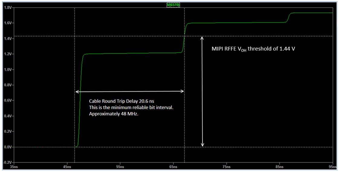
The initial edge voltage is determined by the voltage divider of the DUT’s 100 Ω output impedance and the cable’s 50 Ω characteristic impedance. Because the driver’s impedance is greater than 50 Ω, the initial edge voltage is only 0.6 V, one third of 1.8 V, instead of the desired 0.9 V, one half of 1.8 V. When that edge hits the PXIe-6570 end of the cable, it reflects only up to 1.2 V instead of the desired 1.8 V. That reflected edge then travels all the way back down the cable to the DUT, where some of it reflects off the 50 to 100 Ω impedance mismatch and back to the PXIe-6570 again.
Each reflection back and forth drives the voltage at the receiver (PXIe-6570) further up in a series of stair steps, as shown in Figure 21. If the voltage does not make it all the way to the VOH threshold on the first stair step, it requires a full cable round-trip delay before strobing the signal at the PXIe-6570 and allowing the DUT to drive it back down.
In this case, the cable round-trip delay becomes the minimum bit interval that can work reliably. Frequency is the inverse of the bit interval, so increasing the length of the interconnect slows down the frequency at which you can achieve reliable communication. In reality, it may be somewhat slower than the round-trip delay indicates because of intersymbol interference, noise, or other real-world signal impairments.
If you find your maximum achievable frequency depends on cable length, use your longest cable and check for stair steps on the waveform at the PXIe-6570 digital scope. If you cannot program the DUT to a drive strength close enough to 50 Ω, you cannot check the full voltage thresholds at full speed. Better quality cables do not help; any 50 Ω cable produces the same stair step voltage.
One possible option in this case is to run any voltage threshold tests at much lower speeds and then lower the thresholds to below the first stair step voltage to communicate at full speed.
Figure 21. One option to account for output impedance mismatch effects is to run threshold tests at lower speeds and lower threshold voltages to below the first stair step voltage, which can then be used to run the test at full speed.

