From Saturday, Nov 23rd 7:00 PM CST - Sunday, Nov 24th 7:45 AM CST, ni.com will undergo system upgrades that may result in temporary service interruption.
We appreciate your patience as we improve our online experience.
From Saturday, Nov 23rd 7:00 PM CST - Sunday, Nov 24th 7:45 AM CST, ni.com will undergo system upgrades that may result in temporary service interruption.
We appreciate your patience as we improve our online experience.
This document covers the basics of timing and synchronization in NI-DAQ™mx within the LabVIEW ADE. In particular, topics discussed include taking mixed-mode measurements, synchronizing beyond only analog functionality, and sharing timing signals between data acquisition (DAQ) devices.
Data acquisition in text-based programming environments is very similar to the LabVIEW NI-DAQmx programming as the functions calls are the same as the NI-DAQmx VI's for further information see: Using NI-DAQmx in Text-Based Programming Environments.
There are many applications that require precise control of timing and the ability to synchronize operations. For example, when you’re in charge of measuring and analyzing a large number of highly dynamic signals, any amount of phase mismatch may be unacceptable. There needs to be an understanding that a measurement of one signal at one point in time can be evaluated based on another signal at the same point in time, and thus, these acquisitions need some type of synchronization scheme. NI-DAQmx and the LabVIEW graphical programming environment give you the tools to easily construct these types of data acquisition systems.
NI-DAQmx provides many powerful solutions for your timing and synchronization needs. Its native functionality in LabVIEW demonstrates the next generation of data acquisition programming. Gone are the days of specifically defining wiring paths of signals between devices--NI-DAQmx automatically finds a way to get the signals where you need them. All you have to do is specify the destination. In this sense, the driver intelligently operates behind the scenes to eliminate a complex configuration operation. This, however, is only the tip of the timing and synchronization iceberg...
Since most E Series data acquisition devices have analog input, analog output, counter/timer, and digital input/output functionality, the challenge is often to program the device in such a way as to take advantage of each type of measurement with some amount of certainty that they are synchronized with each other. Some use cases include:
1) Simultaneously Started Analog Input and Analog Output
Operations start simultaneously but are not synchronized
Synchronized Analog Input and Analog Output
Operations can be simultaneously started and set to run at the same rate
Operations can share the sample clock
2) Synchronized Analog Input and Analog Output with a Trigger
Share hardware trigger and sample clock
3) Synchronized Analog and Counter Operations
4) Counter creates pulse train as clock for analog operation
5) Analog clock gates counter operation
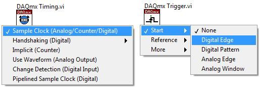
In the NI-DAQmx API, you can use a very small number of VIs to accomplish most of your timing and synchronization needs. In particular, the DAQmx Timing.vi and DAQmx Trigger.vi allow you to specify at what interval your channels should be scanned and when they should start (or stop). By taking advantage of LabVIEW’s polymorphism, these two VIs are capable of defining the timing and triggering of not only analog input signals, but also the aforementioned analog output, counter/timer, and digital input/output (see Figure 1).
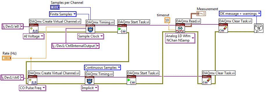
A common use case that demonstrates synchronization concerns is the situation where you would like an analog input and analog output operation to occur using the same clock. In this case, you would need two chains of code: one for analog input and one for analog output. In each, use the DAQmx Timing VI to specify the continuous operation desired. For the analog output timing, leave the “source” input as default – this means your analog output operation will function according to the default analog output clock, which is the internal clock. On the analog input DAQmx Timing VI, all you have to do is specify the “source” to be the analog output sample clock. This sets both analog input and analog output operations to operate on the analog output’s timing signal (see Figure 2).

The previous example demonstrated how you can tie analog timing signals together. What happens when you want to deal with mixed analog and digital signals together? Can you still expect the same amount of seamless integration? The answer is yes.
Imagine that your analog measurements depend upon an external or nontraditional clock signal – ex: take a sample once every millisecond for 10 milliseconds, wait 3 milliseconds, repeat. In this case, you can use the counter functionality on an E Series device to generate the desired timing signal, but how do you tell the analog side to use it as a clock? The answer is, yet again, the DAQmx Timing VI. By specifying your “source” to be a counter’s internal output pin, the counter output will become the analog input clock without the use of an external wire to connect pins on a terminal block (see Figure 3).
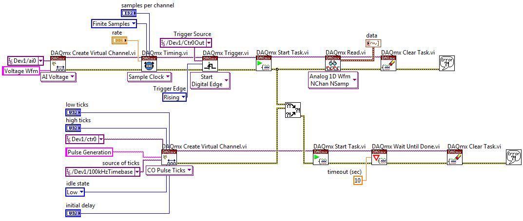
The ease of use demonstrated with synchronization also extends to triggering. Using the DAQmx Trigger VI, you can easily set an operation to wait for either an internal or external trigger signal (analog or digital). A good example of this deals with event triggering. With event triggering, the device ignores the first N triggers before it starts an acquisition. To do this, a counter is used to create the single pulse to start the analog input acquisition. The counter uses the first N triggers to create the low part of the pulse and the valid trigger to start the high part of the pulse and trigger the actual acquisition. In the following example, there are two parallel rows of code; the top configures the analog input operation, and the bottom configures a counter. The source of the trigger is the output of Counter 0, and Counter 0 has been configured to output a trigger pulse after it has input its "nth" pulse. In this case, the 100 kHz internal timebase is selected as the input source, but you could also have specified an external location for the source, allowing you to set up a delayed trigger from an external pulse train (see Figure 4).
Note: In the last two examples, Ctr0InternalOutput and Crt0Out are referenced as the location of a clock or trigger signal. Ctr0Internal Out is a signal available for routes internal to the board. Crt0Out should be used when routing the counter output to PFI and RTSI. The example in Figure 4 could have used CtrOInternal Out instead of Ctr0Out.
To route signals from one location on a device to another like the previous examples demonstrate, you need to take a few things into consideration. First, is NI-DAQmx configured to route these signals? Second, which signals are available for routing? Because the ability to pass these signals relies on an intermediate communication path, make use of the Real Time System Integration (RTSI) bus.
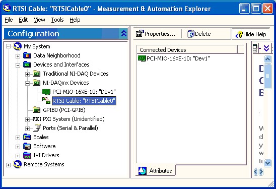
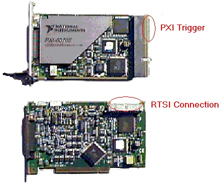
The RTSI bus (available on a PCI device as a 34-pin connector or included in the backplane connector on PXI) exposes 7 pins onto which you can send timing signals from one device to another (or internally on one device). Before you can use this communication path, let the driver know how the devices in the system are connected. For PCI devices, connect the appropriate devices with a RTSI cable and register this connection in Measurement & Automation Explorer (MAX). With MAX 3.0, this is done by right-clicking on NI-DAQmx Devices and choosing Create New NI-DAQmx Device >>RTSI Cable. This will add a RTSI cable to your NI-DAQmx Devices listing. For PXI systems, all you need to do is to identify the PXI system by right clicking on PXI System >> Identify As. The RTSI bus is referred to as the PXI Trigger bus in PXI systems. (Figure 5 shows a RTSI cable connected to one DAQ device.)
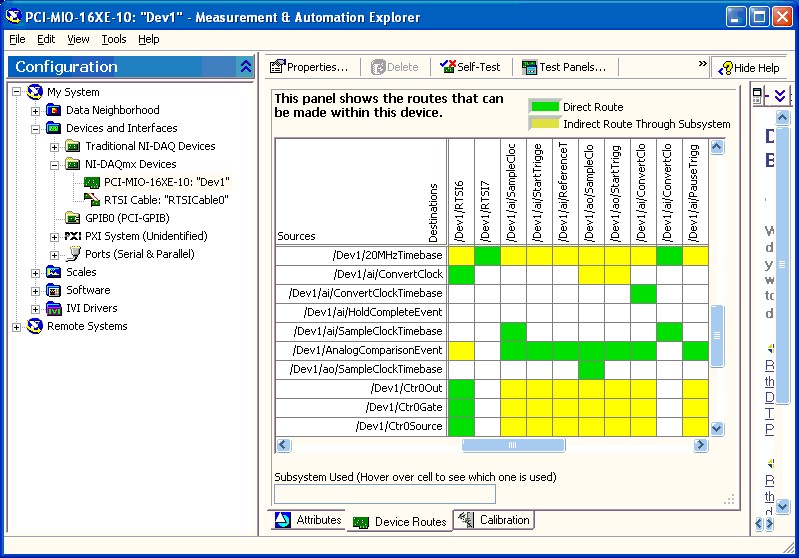
To see which signals can be routed where within a single DAQ device, you can view the Device Routes tab in MAX. When you click on the DAQ device in MAX, you will see the device attributes appear in the window to the right of the Configuration tree. If you choose the Device Routes tab at the bottom of that window, each available signal route is listed. The green squares indicate routes that can be made directly where the yellow squares indicate routes that must go through some type of subsystem on the device to be made. The intermediate subsystems are needed to complete the route are listed in the Subsystem Used box when you hover over a yellow square. This may be useful as indirect routes can sometimes interfere with other operations you are performing (Figure 6).
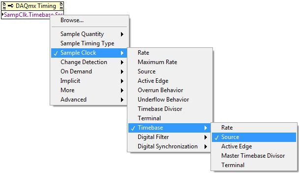
The DAQmx Timing and DAQmx Trigger VIs offer high-level functionality to set up your operation, but there are occasions when lower level information becomes important. Let’s say you need to know what timebase an analog output operation is updating on or for what level an analog edge trigger has been configured. This information is exposed through the DAQmx Timing and DAQmx Trigger Property Nodes (see Figure 7). From these property nodes, you can access all the relevantly configured values, either to set them or view them.
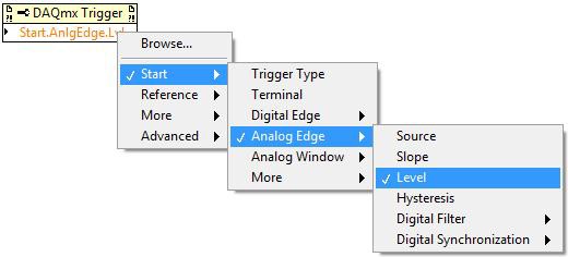
One example of where the DAQmx Trigger Property Node exposes complex functionality is the retriggerable option for counters. In previous APIs, making a counter retriggerable completely changed the code for the counter operation. With the NI-DAQmx API, the simple inclusion of a DAQmx Trigger Property Node, set to Start.Retriggerable, changes the counter from a single trigger to retriggerable operation (see Figure 8).

The previous examples have shown some of the ways you can tie operations together (either through triggering or timing) on the same device. But what if the functionality of one device does not allow the complete characterization of a system? There are certainly times when the sheer channel count of a system requires the combination of multiple devices. If each device contains RTSI connectivity, the same synchronization options are available to us as on a single device.
To show a connection between devices, right-click on the RTSI cable in MAX and select each of the appropriate devices under Add Device to Cable. Once each of the devices has been added, NI-DAQmx will now take advantage of all available routing paths between devices (synchronization will be seamless). If it is a PCI device, you will need to physically add the RTSI cable between the devices.
Now you can reference the appropriate timing or trigger pins from other devices as the "source" of your DAQmx Timing and Trigger VIs. (Management of the RTSI bus is hidden from the user by default, although the option exists to explicitly route certain signals to specific RTSI pins using the Export Signal.vi.) The following example demonstrates how you might share timing signals from one device to another for an analog input operation (see Figure 10).

Note that there are two separate operations taking place here on two separate devices. The sample clock for device one has been configured as the sample clock from device two simply by telling NI-DAQmx to use Dev1/ai/SampleClock as the sample clock for device two. NI-DAQmx figures out how to actually make that route happen to ensure that data will be taken at the same rate on both data acquisition devices.
Most of NI's DAQ devices contain functionality that enables you to share timing and triggering. To take advantage of this functionality, NI-DAQmx, with its characteristic ease of use, simplified analysis, and increased performance, gives you the tools to ensure your measurements occur in the same time domain.