PXIe-5673/5673E Block Diagram
- Updated2024-03-20
- 4 minute(s) read
PXIe-5673/5673E Block Diagram
Refer to the PXI/PXIe-5650/5651/5652, PXIe-5611, and PXIe-5450/5451 block diagram topics for more information about the block diagrams for the individual modules that comprise the PXIe-5673/5673E.


Hardware State Diagram
The following diagram shows the hardware states of the vector signal generator.

- Configuration (Idle)- The device is not generating a waveform. All session properties or attributes can be programmed in the Configuration state. In the Configuration state, the properties or attributes have not necessarily been applied to hardware, and the hardware configuration of the device may not match the session property or attribute values. The device remains configured as it was the last time a session was committed. If the computer has just been powered on, reset, or the niRFSG Reset Device VI or the niRFSG_ResetDevice function has just been called, the device is in the default hardware state.
- Commit (or Aborted)- Applies the device's properties or attributes to the hardware. This state also generates an LO signal for the current settings, commits the AWG, and locks Reference Clocks on only the PXIe-5673/5673E Vector Signal Generator.
- Generation- In the Generation state, the device is generating a waveform as specified by the session properties or attributes configured. Dynamic (or on-the-fly) properties and attributes are applied immediately to hardware. Started Event trigger is generated as the device recognizes triggers. Depending on the configured trigger mode, the device may stay in the Generation state until the generation is aborted.
PXI Trigger Lines
The PXI trigger bus features eight PXI trigger lines.
You can use these flexible lines in a variety of ways:
- To synchronize the operation of several different PXI peripheral devices
- To use one device to control carefully timed sequences of operations performed on other devices in the system
- To pass triggers between devices, allowing precisely timed responses to asynchronous external events that are being monitored or controlled
The number of triggers that an application requires varies with the complexity and number of events involved.
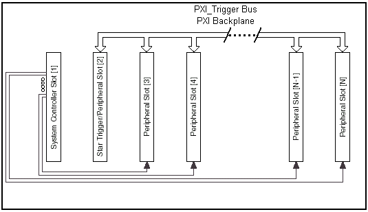
The PXI Specification is implemented with the RTSI bus through the PXI trigger lines. PXI Specification requires eight lines, PXI_Trig<0..7>, on the P2/J2 connector of the PXI chassis for the trigger lines.
System Reference Clock
The PXI chassis supplies the PXI 10 MHz system Reference Clock signal (PXI_CLK10) and the PXI 100 MHz system Reference Clock signal (PXIe_CLK100), which is phase synchronous with the PXI_CLK10 signal, independently to each peripheral slot.
An independent buffer drives the clock signal to each peripheral slot. The buffer has a source impedance matched to the backplane and a skew ranging from less than 1 ns to better than 250 ps between slots. You can use this common Reference Clock signal to synchronize multiple devices in a measurement or control system. You can drive PXI_CLK10 from an external source through the PXI_CLK10_IN pin on the P2 connector of the PXI star trigger slot, which is Slot 2. Sourcing an external clock on this pin automatically disables the 10 MHz source on the backplane. You can synchronize multiple chassis that have connectors on the back panel for 10 MHz reference in and 10 MHz reference out. Refer to your PXI chassis documentation for more information.
PFI Lines
PFI lines are multipurpose programmable function input/output lines. These lines serve as connections to virtually all internal timing signals. NI RF signal generators have up to six digital lines that can accept or generate a trigger, generate a marker, accept or generate a Reference Clock. The function of each PFI line is independent.
Routing Signals
To export signals to the PFI lines on the device front panel, you must specify a trigger, clock, or event using the signal parameter of the niRFSG Export Signal VI or the niRFSG_ExportSignal function.
To import signals, you must select a trigger using a polymorphic instance of the niRFSG Configure Trigger VI and specify a PFI line as the source terminal.