Advantages of Xilinx 7 Series FPGA and SoC Devices
Overview
NI LabVIEW FPGA hardware targets use Xilinx FPGA and SoC technology to help engineers and scientists create custom, reconfigurable systems with onboard processing to solve complex control and measure challenges and get to market faster at lower overall costs. NI FlexRIO, R Series, PXI, CompactRIO, Single-Board RIO, System on Module (SOM), myRIO, and other products now feature Xilinx 7 series FPGAs and SoCs. Additionally, with LabVIEW 2014 and later, developers using 7 series also benefit from Vivado, the latest and fastest compilation technology from Xilinx. As a LabVIEW FPGA user, you gain these benefits without needing to learn how to use Vivado as it is fully integrated into the NI tool chain.
Contents
- Introduction to 7 Series FPGAs
- Zynq-7000 SoCs: The Benefits of CPUs and FPGAs on a Single Device
- Kintex-7: The Right Mix of High Performance and Power Savings
- Artix-7: The Value of a Smaller Size, Lowest Power Consumption, and Performance
- Xilinx Vivado: Improved Compilation Performance
- Additional Resources
Introduction to 7 Series FPGAs
Xilinx expanded the definition of FPGAs at the 28 nm node and delivered not only the industry’s most advanced FPGAs but also a game-changing line of SoC and 3D ICs. NI played a key role in helping define the requirements for Xilinx 7 series devices and was a lead partner in the SoC program.
Rather than use the high-performance/high-power process tailored for graphics chipsets in PCs or the low-power process targeted to mobile phone devices, Xilinx worked with TSMC to develop a process tailored to the requirements of devices. Thus, the TSMC 28 nm high performance low power (HPL) process technology includes the right mix of performance and power savings for all the markets Xilinx devices serve. Designs that need to run at high performance do not have to come at an extreme cost of higher power consumption. Conversely, designs that need to meet strict power requirements can still achieve relatively high-performance goals. With the entire 7 series portfolio targeting the same 28nm HPL silicon process, Xilinx concentrated on architecture innovation. For the 7 series, Xilinx introduced a full line of scalable FPGAs, which includes a new low-cost Artix-7 family, a midrange Kintex-7 family, and a high-end Virtex-7 family. The base FPGA building blocks of logic cells, DSP blocks, BlockRAM, and so on are all consistent across the 7 series, making it much simpler to migrate designs.
In addition to creating a full line of FPGAs, Xilinx innovated two first-of-their-kind devices: the Zynq-7000 SoC and the Virtex-7 3D ICs. Both devices have won numerous innovation awards from trade publications and industry associations across the globe.
Zynq-7000 SoCs: The Benefits of CPUs and FPGAs on a Single Device
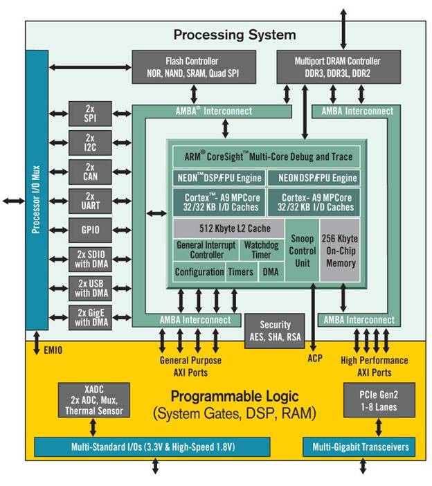
As shown in Figure 1, the Zynq-7000 SoC combines, on a single chip, dual-core ARM Cortex-A9 CPUs with a rich set of standard I/O peripherals and a multi-ported memory controller in an SoC Processing System domain with FPGA fabric in a Programmable Logic domain. Over 2,000 interconnects interface the Processing System to the Programmable Logic. This provides the high-performance, low-latency communication, extension, flexibility, and capability between processing and programmable logic that other systems connecting discrete processor-based devices to FPGAs through printed circuit boards cannot achieve. This integration is a key value for NI platforms based on Zynq-7000, including the CompactRIO cRIO-906x, Single-Board RIO products (sbRIO-9607/9627/9637), Single-Board RIO GPIC kits for power electronics control systems, System-On-Module (SOM) sbRIO-9651, myRIO, and the Grid Automation System. The high-performance, low-latency interconnect between the Processing System and the Programmable Logic enables 16 parallel DMA channels and functional bandwidth of over 300 MB/s.
All the devices in the 7 series standardized on using the ARM AXI-4 bus protocol. IP created for implementation in ARM-based systems can easily be migrated into any 7 series device. With LabVIEW FPGA, NI provides a set of application-specific IP as well as access to Xilinx CORE Generator IP standardized on the AXI interface. This provides IP interoperability across vendors and makes it easier to maintain and improve designs over time.
Figure 1: The Zynq-7000 SoC marries a dual-core ARM Cortex-A9 Processing System, 28 nm FPGA fabric (Programmable Logic), and key peripherals on a single device.
Kintex-7: The Right Mix of High Performance and Power Savings
Xilinx invented the FPGA in 1988 and has delivered state-of-the-art FPGA technology ever since. The Kintex-7 represents the pinnacle of that technology. The device family features a perfect balance of FPGA fabric clock rate performance versus power consumption, high-speed I/O, capacity, security, and reliability.
This highly balanced feature set makes the device well suited to serve a broad number of test and high-performance embedded applications, such as custom triggering, hardware-timed test sequencing, medical imaging, big physics control and monitoring ultra-wide bandwidth communications and radar, signal intelligence, protocol-aware digital test, real-time vision algorithms, and software defined radio.
The new Kintex-7 FPGAs are ideally suited for many products that use the LabVIEW reconfigurable I/O (RIO) architecture. This device family has the capacity and performance of previous high-end FPGAs, but at half the power consumption. The impressive reduction in power means devices can pack more than twice the digital signal processing capability per device as the previous generations of FPGA-enabled hardware from NI. With this increase in logic and DSP resources, engineers can implement more complex algorithms with more extensive use of signal processing and real-time analysis, and address the growing I/O data rates and complexity of today’s applications.
In addition to more DSP resources, the DDR3 memory controller has helped NI implement a 10 GB/s (theoretical) interface to temporary storage compared to the previous-generation rates of 3.2 GB/s. Furthermore, the built-in PCI Express controller bandwidth increased from 800 MB/s to 1,600 MB/s, enabling even faster data transfers from the FPGA to the host.
NI platforms and products that capitalize on Kintex-7 advantages include R Series multifunction RIO, PXI Platform, FlexRIO, Digital I/O, CompactRIO platforms , and USRP (Universal Software Radio Peripheral)platforms (Software Defined Radio).
Artix-7: The Value of a Smaller Size, Lowest Power Consumption, and Performance
Artix-7 uses the same FPGA resources as Kintex-7, but optimized for even lower power consumption and smaller size packages, delivering similar advantages, but at the value-line price point. Artix-7 FPGA technology is used in NI products with the Zynq-7000 SoC as well as in C Series expansion chassis for implementing custom timing, onboard processing, and control. Because the FPGA building blocks are functionally identical to Kintex-7, migration between devices, especially when using LabVIEW FPGA, is readily accomplished.
Xilinx Vivado: Improved Compilation Performance
In LabVIEW 2014 and later, developers using Xilinx 7-series FPGAs and Zynq-7000 SoCs in their NI RIO hardware can also benefit from Vivado, the latest compilation technology from Xilinx. Vivado compilation tools offer numerous benefits including:
- More consistent, reliable timing closures
- Improved resource utilization
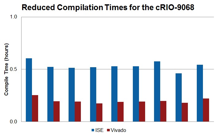
- Faster compiles for Kintex-7 FPGA targets previously using Xilinx ISE (NI cRIO-9068 and NI PXIe-7975R)
Figure 2: New Vivado compilation technology from Xilinx offers reduced compilation times for Kintex-7 and Zynq-7000 SoC targets previously using Xilinx ISE.
Author Information
Robert Bielby—Senior Director of Strategic Marketing and Business Planning, Xilinx Inc.
Greg Brown, Principal Marketing Manager, NI
Additional Resources
Explore NI targets and devices that use Xilinx 7 series FPGAs and SoCs:
- CompactRIO
- Single-Board RIO
- FlexRIO
- PXI platforms
- USRP platforms
- Learn about the LabVIEW RIO architecture and LabVIEW FPGA: LabVIEW FPGA

