NI-DAQmx Synchronization of PXI Express Modules
Overview
One of the most important aspects of a sensor measurement system is the degree to which you can correlate in time the data acquired from multiple channels. If your data is not appropriately correlated in time, or synchronized, then your analysis and conclusions from your test data are inaccurate. NI has designed NI SC Express devices to ensure high-performance synchronization. The following sections explain the synchronization concepts and how you can take advantage of them.
Contents
- PXI Platform and SC Express Synchronization Overview
- Synchronization General Concepts
- Synchronization Approaches and Options
- Digital Filter Group Delay
- SC Express Flexible Synchronization
- Additional Resources
PXI Platform and SC Express Synchronization Overview
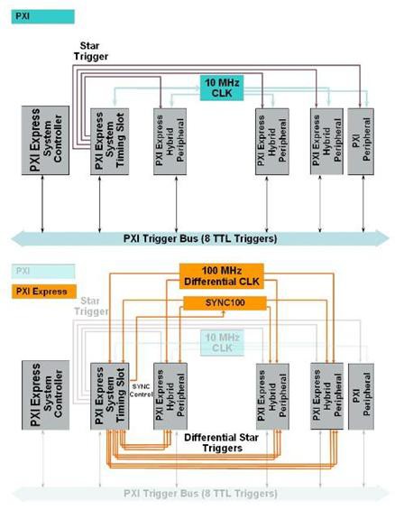
As the latest evolution of the PXI platform, PXI Express has been designed to deliver a higher degree of synchronization to measurement I/O devices while remaining backward-compatible. PXI Express maintains the 10 MHz backplane clock as well as the single-ended PXI trigger bus and PXI star trigger signal provided by the original PXI specification. PXI Express also adds a 100 MHz differential clock and differential triggers to the backplane, providing increased noise immunity and industry-leading synchronization accuracy.
The 100 MHz differential clock in the PXI Express backplane allows multiple devices to base their sample clocks on the same reference. With the backplane trigger lines, you can coordinate the triggering of all the devices in the chassis to the same 100 MHz clock edge.
Figure 1. PXI Express timing and triggering buses add a differential system clock, differential signaling, and differential star triggers on the backplane
As with previous PXI chassis, a timing and synchronization module can replace the backplane clock with a higher-precision timebase in a single PXI Express chassis or it can be used to synchronize measurement devices in multiple PXI Express chassis. If the application requires you to synchronize multiple chassis over large distances, then GPS or IRIG-B PXI timing modules can synchronize the chassis by a common clock signal.
NI has enhanced the DAQmx driver with an innovative approach to configure multiple SC Express modules for synchronization. A full chassis of any single SC Express module type can be programmed with one multidevice task. With multidevice tasks, you can scale your application from one to 544 channels using the same DAQmx code. You can also use a single DAQmx task to automatically synchronize channels across multiple boards with different measurement types, as shown in Figure 2.
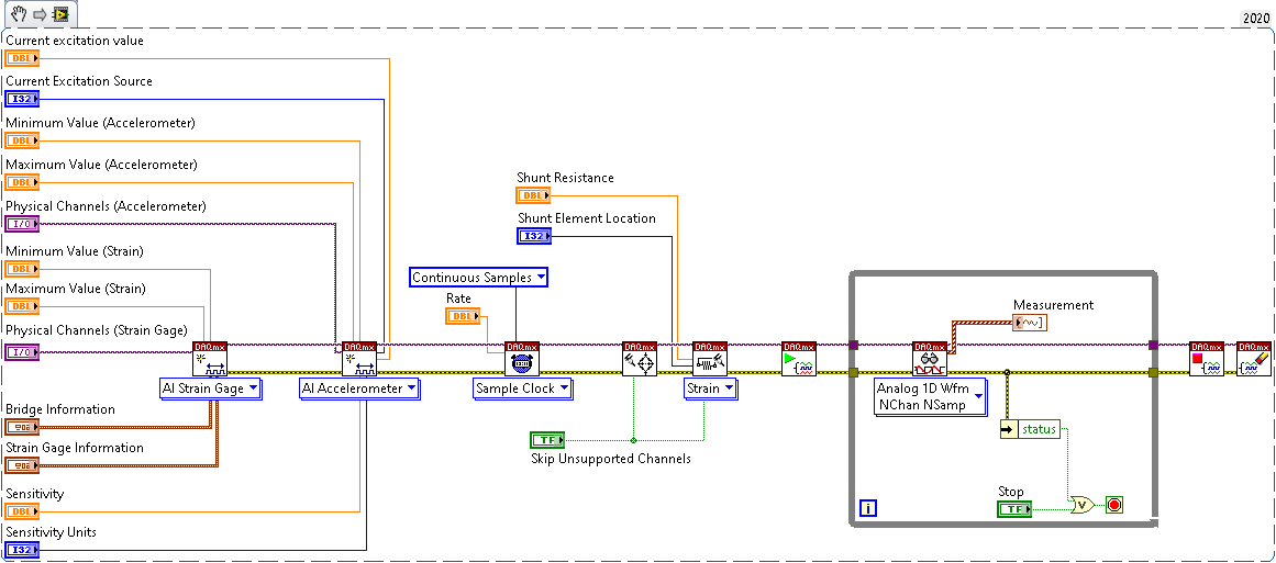
Figure 2. Example LabVIEW Code for Acquiring Multiple Modules with Different Measurement Types
When programmed in this way, the SC Express modules use the PXI Express chassis 100 MHz differential clock as a reference clock and the backplane trigger lines to coordinate starting acquisitions for synchronization. Examples of supported multidevice tasks configurations are shown in Table 1, as you can see the SC Express modules deliver strong synchronization performance. For details on DSA, SC Express, and X Series multidevice task combinations supported by a specific release of NI-DAQmx, refer to the DSA, SC Express, and X Series Multidevice Tasks topic in the NI-DAQmx Help.
SC Express Support for Multidevice Tasks | Module-to-Module Skew |
|---|---|
NI PXIe-4300: High-Voltage Analog Input Module | <50 ns |
NI PXIe-433x: Bridge Input Modules | <150 ns |
Table 1. Synchronization Performance with Multidevice tasks
Synchronization General Concepts
This section describes background concepts related to synchronization. It is helpful to understand these concepts prior to designing a synchronized measurement application.
Synchronization Terms
Triggers: A trigger is a command that controls an acquisition. You can use triggers to start, stop, or pause an acquisition. Trigger signals may originate from either software or hardware sources.
Clocks: Clocks are periodic digital signals used to time the acquiring of data. Depending on the context, you may use a clock signal to directly control the data acquisition or as a reference timebase to derive another clock.
Asynchronous Inputs: An asynchronous input is an input whose timing relationship with respect to the clock signal used to receive the input is unknown, such as an external digital trigger received by the onboard clock of a device. Other examples include a software command or an analog trigger event. An asynchronous input may be detected either before or after a clock edge. If it occurs too close to a clock edge, then you cannot tell whether it is detected before or after the clock edge.
This is not a problem when a single device receives the input. However, if the same asynchronous input is fed to multiple devices, then they may detect the input change on different clock edges. This results in the operation of the devices being unsynchronized, even if the devices share the same clock. The way to fix this problem is by using master-slave synchronization.
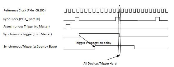
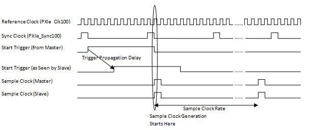
Master-Slave Synchronization: Master-slave synchronization is also referred to as trigger skew correction in NI-DAQmx documentation. This method works by designating one master device to receive an asynchronous trigger input. This master device then drives the trigger to all the slave devices in a synchronous fashion. The trigger driven from the master device to the slave devices is synchronous to a common timing reference clock. As a result, all devices can reliably detect that trigger event on the next edge of the reference clock.
The following waveforms illustrate this concept:
Figure 3. Master-slave synchronization
This results in the precise synchronization of both the master and slave devices. One side effect of this scheme is that it leads to a latency of one to two reference clock periods that are required to resynchronize and send the trigger.
Note that the reference clock used for master-slave synchronization depends on the application. In some cases, the backplane PXIe_Sync100 signal is used for this purpose. In other cases, a different common reference shared by all the devices being synchronized may be used (for example, a sample clock).
Synchronization Signal Connections
You can choose from many different ways to share clock and trigger signals between devices in a PXI Express chassis. You can share signals via external wiring (many devices provide input pins for this purpose) or via the PXI Express backplane trigger bus. The mechanism you use to share your clock and trigger signals affects the synchronization accuracy.
| Signal | PXI Express Only? | Requires System Timing Controller Module? | Device-to-Device Skew | Signal Integrity |
|---|---|---|---|---|
| PXIe_Clk100 | Yes | No | <250 ps | Best |
| PXIe_DStar<A..C> | Yes | Yes | <500 ps | Best |
| PXI_Clk10 | No | No | <1 ns1 | Better |
| PXI_Star | No | Yes | <10 ns | Better |
| PXI_Trig<0..7> | No | No | <80 ns | Fair |
| External Wiring | No | No | Variable | Variable |
1There may be up to 6.5 ns of skew between PXI_Clk10 and PXIe_Clk100. So, while a set of devices using PXI_Clk10 as a reference clock will have little skew between them, these devices may see up to 6.5 ns of skew when compared to other devices using PXIe_Clk100 as a reference clock.
Table 2. The PXI Express differential Clk100 and DStar trigger signals have the tightest levels of synchronization and the best signal integrity.
You can achieve the best synchronization performance when using clock signals distributed via PXIe_Clk100, PXIe_DStar<A..C>, PXI_Clk10, or PXI_Star. The PXI_Trig<0..7> bus is a shared bus connected to each module in the backplane. It is extremely useful because it provides many connections for triggering between the devices. However, as a result, these signals are heavily loaded, causing long propagation delays. The propagation delays vary depending on the position of the devices within the backplane. In addition, the signal integrity (the quality of the clock rising and falling edges) is also quite variable depending on the number and type of modules installed in the backplane, the positions of those modules, and the specific hardware used to drive the PXI_Trig bus from the modules. Side effects of poor signal integrity can include additional noise and jitter on these signals. In extreme cases, it is possible for a single edge on a signal to end up looking like two separate edges, resulting in double-clocking. Therefore, NI recommends that the PXI_Trig<0..7> lines be used are exclusively for routing trigger signals.
Synchronization Approaches and Options
To understand how different PXI Express devices synchronize, you need to know the underlying architecture of these different types of devices. Broadly speaking, there are two main classes of devices from a synchronization perspective:
- Sample clock timed devices
- Oversample clock timed devices
Sample Clock Timed Devices
A sample clock is a signal that controls the point in time at which samples are acquired. Sample clock timed devices use analog-to-digital converters (ADCs) that are able to immediately initiate a conversion in response to a clock edge at any given time. An example is a successive approximation register (SAR) ADC that typically has a dedicated convert line that can be toggled to trigger an immediate conversion. As a result, these types of devices offer extensive flexibility in terms of their clocking. The ADC is able to perform a conversion off virtually any clock signal, including variable frequency or nonperiodic signals, up to the maximum rate supported by the device.
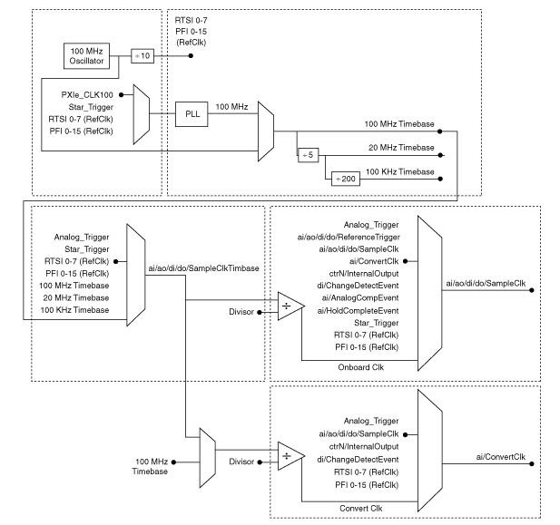
NI devices in this class provide flexible timing engines capable of driving the convert line on their ADCs from a variety of sources. For example, the following block diagram shows the different sources that can feed the AI sample and convert clocks on NI X Series devices:
Figure 4. NI sample clock timed devices provide flexible timing engines capable of driving the convert line on their ADCs from a variety of sources.
Key signals shown in Figure 4:
- Sample clock: This signal directly initiates a set of measurements on all the channels in your task. Each sample clock edge causes all of these channels to be converted a single time.
- Convert clock: This signal applies only to multiplexed devices, where a single ADC is shared among multiple channels. The convert clock signal initiates a single ADC conversion on a single channel. Depending on the number of channels being acquired, the convert clock signal needs to assert one or more times per sample clock edge.
- Sample clock timebase: A clock signal that can be divided down to create the sample clock.
- Convert clock timebase: A clock signal that can be divided down to create the convert clock.
From Figure 4, you can see how much flexibility you have in controlling the acquisition timing of these types of devices. They can acquire from their onboard timebases (for example, a 100 MHz oscillator), from backplane clocks and triggers (for example, PXIe_Clk100, star trigger, RTSI<0..7>), from other onboard subsystems (for example, AI sample clocks can come from AO, DI, DO, or counter operations), from analog comparators, or from external digital inputs (for example, PFI lines).
Examples of NI data acquisition devices that are sampled clock timed include the following:
- All NI E Series, M Series, and X Series devices
- NI PXIe-4300 and PXIe-4353 SC Express devices
Methods for Synchronizing Sample Clocks
To synchronize these devices, you must ensure that the sample clock signal is synchronized across all the devices. There are different ways to achieve sample clock synchronization, each of which features different pros and cons.
Share Sample Clock Directly (Sample Clock Synchronization)
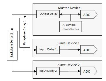
The most basic method for synchronizing sample clock signals is to take the sample clock from one of the devices (the master device) and route it directly to the other devices (the slave devices). There are several types of delays that can cause skew with this synchronization method.
Figure 5. Sample clock synchronization is the most basic method but there are several types of delays that can occur.
When the master outputs the sample clock to the backplane, a small amount of skew develops between the output sample clock and its internal sample clock due to the output delay. The output sample clock signal is then routed to the slave devices via the backplane trigger lines. The delay associated with this routing depends on the path the signal takes on the backplane. If the sample clock is routed via the PXI_Trig lines, this delay may be up to ~80 ns. If it is routed via the PXI_DStar lines, the delay may be much lower. When the sample clock is received by the slave devices, additional skew results, depending on the different input delay values for each device.
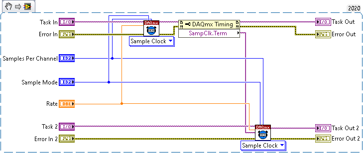
Figure 6. You can use the sample clock of a master device to synchronize multiple slave devices.
The VI, "Get Full Terminal Name.vi" can be found at <LabVIEW>\examples\DAQmx\Synchronization\SubVIs\Get Full Terminal Name.vi or it can be found listed as a download for this article.
To perform sample clock synchronization:
- Configure all devices to use sample clock timing.
- Set the source of the sample clock on all slave devices to the internal sample clock terminal from the master device.
| Pros | Cons |
|---|---|
|
|
Table 3. Pros and Cons to the Sample Clock Synchronization Method.
Derive Sample Clock from a Common Reference Clock (Reference Clock Synchronization)
This method provides a common reference clock to all devices, which then divide down the reference clock to generate a sample clock. Reference clock synchronization offers the most accurate synchronization possible between supported devices.
In PXI Express, the reference clock is typically PXIe_Clk100. It is a common differential 100 MHz clock that is available to each slot in the backplane with subnanosecond skew. To synchronize the sample clocks, a trigger signal is sent from the master device to the slave devices telling them to start generating sample clocks. However, it is not possible for the trigger to propagate all the way from the master to the slave devices within a single 10 ns PXIe_Clk100 period. To overcome this limitation, triggers are sent and received synchronously with PXIe_Sync100, which is a slower 10 MHz (100 ns) clock signal. The master outputs the start trigger signal synchronously with one PXIe_Sync100 pulse, and then all devices start on the next PXIe_Sync100 pulse after the trigger is received. This is referred to as trigger skew correction in the NI-DAQmx Help.
Figure 7. The master outputs the start trigger signal synchronously with one PXIe_Sync100 pulse, and then all devices start on the next PXIe_Sync100 pulse after the trigger is received.
Although the under-the-hood details of reference clock synchronization are complex, NI-DAQmx makes using this sophisticated synchronization technique easy. NI-DAQmx automatically performs reference clock synchronization (along with trigger skew correction) on supported devices anytime you create a multidevice task. This means that acquiring synchronized data from multiple devices is as simple as acquiring data from a single device.
In addition, you can manually perform this process by specifying PXIe_Clk100 as the reference clock for both devices and then configuring the slave device to use the start trigger generated by the master device.

Figure 8. You can manually perform this process by specifying PXIe_Clk100 as the reference clock for both devices and then configuring the slave device to use the start trigger generated by the master device.
| Pros | Cons |
|---|---|
|
|
Table 4. Reference clock synchronization offers the most accurate synchronization possible between supported devices.
Share Trigger Signal Only
You can loosely synchronize devices by sharing a trigger signal only – without sharing a common sample clock or reference clock. In this case, all devices start at roughly the same time due to the common trigger signal. However, the devices then drift during the acquisition because their respective sample clocks are not locked together.
Figure 9 illustrates synchronization via a common trigger signal. Note that the sample clock signals generated by the two devices start off skewed from each other due to the amount of time that it takes for the trigger signal to propagate between the devices. In addition, over time the sample clock signals drift further apart if the sample clocks are not derived from a common reference clock.
Figure 9. You can loosely synchronize devices by sharing a trigger signal only.
To share a trigger signal in NI-DAQmx, you can specify the desired trigger signal as the “source” input to the NI-DAQmx Trigger VI.
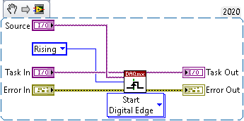
Figure 10. You can share a trigger signal with NI-DAQmx driver software.
| Pros | Cons |
|---|---|
|
|
Table 5. Synchronization with only a trigger signal may be acceptable for short acquisitions.
Control the Convert Clock on Multiplexed Device
Multiplexed devices have an AI convert clock that initiates ADC conversion for each sample from a single channel. For example, if you acquire two samples across three channels on a multiplexed device, you may have timing similar to Figure 11.
Figure 11. The AI convert clock initiates ADC conversion for each sample on multiplexed devices.
With some multiplexed devices (for example, E Series, M Series, and multiplexed X Series), you can directly control the AI convert clock timing. For these devices, you have similar flexibility on controlling the AI convert clock as you have in controlling the AI sample clock. You can import or export this signal as well as control the AI convert clock from either internal or external timing sources.
Other multiplexed devices (for example, the NI PXIe-4353) prevent you from directly controlling the AI convert clock timing. On these devices, you cannot import or export an AI convert clock signal. Instead, this signal is always driven based on an internal timebase. However, you may still be able to use these devices to select different ADC timing modes. With these modes, you can indirectly alter the AI convert clock timing. For example, a high-resolution timing mode might result in a slow AI convert clock in conjunction with more accurate AI data, while a high-speed timing mode might result in a faster AI convert clock at the expense of less accurate data.
Refer to your specific hardware documentation for complete details regarding AI convert clock timing control.
Oversample Clock Timed Devices
This category of devices uses a free-running oversample clock to drive the ADC conversion process. This clock signal must always be running to keep the ADC operating. The ADC itself produces a sample at a divided-down rate of the oversample clock. These devices typically use high-speed delta-sigma converters.
Some devices (for example, the NI PXIe-4353) use a delta-sigma ADC, but they use it in a mode where the ADC is reset by an external convert line prior to each conversion. As a result, such devices fall into the sample clock timed device class even though they use delta-sigma ADCs.
Oversample clock timed devices are less flexible in terms of their clocking. Because the ADC requires a free-running oversample clock, these devices cannot be directly run off external signals, such as encoders. Also, they cannot act as slave devices receiving an arbitrary sample clock signal.
Examples of oversample clock timed devices include the following:
- All dynamic signal analysis (DSA) devices (NI 446x, NI 447x, NI 449x)
- NI PXIe-433x bridge input modules
Oversample clock timed devices synchronize with each other using either reference clock synchronization or sample clock timebase synchronization.
Reference Clock Synchronization
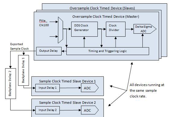
To understand how reference clock synchronization works for oversample clock timed devices, you need to know about the timing and synchronization circuitry on these devices.
The delta-sigma ADCs used on these devices require a free-running oversample clock to drive their ADC conversion process. The ADC produces a new sample after a certain number of oversample clock periods have elapsed. The number of clock periods required to produce a new sample is called the oversample rate. For example, an ADC with an oversample rate of 256 produces data at a 50 kS/s rate if it is provided with a 12.8 MHz clock. If you want to acquire data at 30 kS/s, you have to provide the ADC with a 7.68 MHz clock.
Figure 12. Diagram of Oversample Clock Timed Devices
To offer users flexibility in choosing their sample rates, these devices feature agile direct digital synthesis (DDS) clock generator circuitry that can generate the required ADC oversample clock for a wide range of desired sampling rates.
Reference clock synchronization for these devices works in two stages:
- Stage 1. Reset the DDS clock generator, clock divider, and ADCs on all the devices such that the sample clocks on all the devices are synchronized.
- Stage 2. Start the acquisition synchronous to the sample clocks on all the devices.
Before jumping into the complicated details of how this all works, remember to keep the following in mind:
- NI-DAQmx automatically handles everything required to perform reference clock synchronization on supported devices anytime you create a multidevice task.
- Even if you are an advanced user trying to manually control this synchronization process, you should probably use the NI-DAQmx programming examples as a starting point for your application.
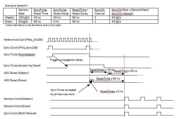
Figure 13 shows how you perform the first stage of reference clock synchronization. This scheme works by locking all devices to a common reference clock (PXIe_CLK100). A synchronization pulse is then sent from the master device to all the slave devices synchronous to the PXIe_Sync100 signal. After receiving the synchronization pulse, all the devices then wait until the next edge of PXIe_Sync100. At this point, all the devices simultaneously begin the process of resetting their DDS clock generator circuits, clock divider circuits, and ADCs. This entire reset process takes a while – the specific time that it takes is reported by NI-DAQmx via the SyncPulse.ResetTime property. To line up multiple devices with different reset times, add another SyncPulse.ResetDelay value to faster devices to align them with slower devices. This results in a common ResetTime+ResetDelay value for all devices, which means that all the devices produce their first sample clock pulse at the same point in time.
In addition, you can synchronize devices running at different rates by modifying the SyncClk.Interval property. The SyncClk is a clock signal used when sending triggers between devices. Triggers are sent on one SyncClk edge and received on the next SyncClk edge. The SyncClk is set to run at the same rate on all devices even if those devices are running at different sample clock rates. If all devices are running at the same rate, then the SyncClk.Interval = 1, and the SyncClk rate is the same as the sample clock rate.
Figure 13. Lock all devices to a common reference clock and send a synchronization pulse to all slave devices.
The following block diagram shows an example of how you can program these parameters in NI-DAQmx for a PXIe-433x. Note that this example also sets an extra parameter called MinDelayToStart. This is just a software feature to ensure that the master device waits long enough after sending the sync pulse before attempting to start the acquisition.
Note that this example may not be available for all versions of DAQmx and that it is important to check what functionality is available for the driver version and device. For further reference consult the following articles:
- Timing and Synchronization Features of NI-DAQmx
- Synchronizing Different Types of DSA Devices at Different Rates

Figure 14. You can synchronize devices running at different rates by modifying the SyncClk.Interval property.
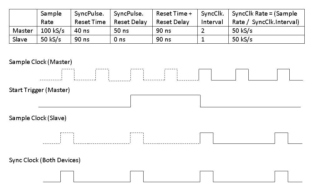
Now that Stage 1 (sample clock synchronization) is complete, Stage 2 (starting the acquisition) is simply a matter of sending out a start trigger synchronous to the sync clocks on all devices.
Stage 2 begins with the master sending out a start trigger. This start trigger is output synchronously to the sync clock, which was previously synchronized on all the devices. After all the devices receive the start trigger, they wait for their next internal sync clock. At this point, all devices begin generating their sample clocks at essentially the same time. Note that internal to both the master and slave devices there is a sample clock that is running behind the scenes. Data associated with this sample clock is not acquired (and the sample clock signal is not output to other devices) until the start trigger event has occurred. This is represented on the waveforms by the dashed lines for the sample clock signal prior to the start trigger occurring.
Figure 15. After the master sends out a start trigger, all devices begin their sample clocks at the same time.
Sample Clock Synchronization
Sample clock timebase synchronization is used by some older PCI and PXI DSA devices (for example, NI 446x and NI 447x devices). Newer PXI Express-based devices support reference clock synchronization. For details on sample clock timebase synchronization, refer to the NI-DAQmx Help or DSA User Manual.
Synchronizing between Sample Clock and Oversample Clock Timed Devices
Export Sample Clock from Self-Timed Devices
This method involves exporting the sample clock signal from the oversample clock timed devices. You may have multiple oversample clock timed devices in this scheme, all of which are synchronized via reference clock synchronization. You synchronize sample clock timed devices by exporting a sample clock signal from the oversample clock timed devices to the sample clock timed devices via the PXI Express backplane. In this case, the sample clock timed devices are using the sample clock synchronization method described earlier.
Figure 16. Multiple oversample clock timed devices are all tightly synchronized using reference clock synchronization with the PXIe_Clk100 signal
In this example system, multiple oversample clock timed devices are all tightly synchronized using reference clock synchronization with the PXIe_Clk100 signal. One of these devices then generates a sample clock that is routed via the PXI Express backplane trigger lines to one or more sample clock timed slave devices. The amount of skew between the slaves depends on the skew in the backplane routing delays .
The NI-DAQmx code required to route this sample clock to the sample clock timed slave devices is exactly the same as the sample clock synchronization code shown previously.

Figure 17. The top task contains the oversample clock timed master device that generates the sample clock, and the bottom task contains the sample clock timed slave devices receiving this sample clock.
The VI, "Get Full Terminal Name.vi" can be found at <LabVIEW>\examples\DAQmx\Synchronization\SubVIs\Get Full Terminal Name.vi or it can be found listed as a download for this article.
In this case, the top task contains the oversample clock timed master device that generates the sample clock, and the bottom task contains the sample clock timed slave devices receiving this sample clock.
| Pros | Cons |
|---|---|
|
|
Table 6. This method allows synchronization across different types of devices.
Share Triggers Across Sample Clock Timed and Oversample Timed Devices
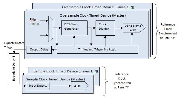
You can use this same technique to synchronize oversample clock and sample clock timed devices as described previously. One advantage of using this technique is that you can separate your devices into two groups: sample clock timed and oversample clock timed. You can then use reference clock synchronization within each group to achieve tight synchronization within the group. Then you can share a trigger signal between the two groups to start them both at roughly the same time.
Figure 18. You can use reference clock synchronization within the sample clock timed group and over sample clock timed group.
As you can see, there is still some skew between each of the two groups due to the time it takes for the trigger signal to propagate across the backplane as well as the time required for the receiving device to resynchronize and accept the trigger signal. However, within each group there is virtually zero skew due to reference clock synchronization. Also note that because you are sharing only a trigger signal (and not the sample clock directly), each of these groups can now run at different rates.
| Pros | Cons |
|---|---|
|
|
Table 7. This method allows sample clock timed devices to run at a different (potentially faster) rate than the oversample clock timed devices.
Trigger Signal Synchronization Caveats
Caveat 1: Trigger Skew
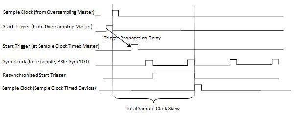
You need to consider a couple of advanced caveats when synchronizing via trigger signals. First, you see skew between the devices due to the time it takes for the trigger signal to propagate to the destination device. In addition, you must synchronize this trigger signal to the acquisition clock by the slave device. This results in potentially significant skew. The waveform in Figure 19 illustrates this skew (assuming that multiple sample clock timed devices are receiving a start trigger from multiple oversample clock timed devices):
Figure 19. You must synchronize the trigger signal to the acquisition clock to minimize skew.
Note that when the trigger is received by the sample clock timed master, the master must resynchronize this trigger to the synchronization clock and forward the trigger onto all the slave sample clock timed devices. This is the trigger skew correction process discussed earlier. As a result, the sample clock for the two sets of devices is skewed by between one and two synchronization clock periods. In this example, the synchronization clock used is the PXIe_Sync100 signal. Because the PXIe_Sync100 has a 100 ns period, the sample clock for the two sets of devices is skewed by between 100 and 200 ns.
However, if you repeat this process, but instead send the start trigger from the sample clock timed devices to the oversample clock timed devices, you end up with much more skew. The reason for this is that the oversample clock timed devices have a free-running sample clock in the background. They are unable to immediately respond to a trigger signal, and must wait for the next sample clock. In this case, the sync clock shown in Figure 19 becomes the sample clock signal internal to the oversample clock timed devices. This results in a skew of between one and two sample clock periods occurring between the two groups of devices. This is a much greater source of error.
Note that in either case, you may be able to measure the actual value of this skew by using a counter to perform a two-edge separation measurement between the sample clock signals exported by each group of devices.
Caveat 2: DDS Clock Drift
Intuitively, you expect that if both the sample clock timed devices and the oversample clock timed devices are both locked to the exact same reference clock (PXIe_Clk100), there should be zero drift between the two sets of devices. In some cases, at certain rates, it may be true that there is exactly zero drift between the devices.
However, this is not always the case. The DDS is usually programmed with a 32-bit tuning word controlling how the PXIe_Clk100 signal is divided down to produce the oversample clock for the delta-sigma ADCs used on these devices. Sometimes, when calculating this tuning word, there is a small rounding error that forces you to set this tuning word to be ≤0.5 bits higher or lower than the ideal value. This can result in an extremely small error between the sample clock rate of the oversample clock timed and sample clock timed devices. This error is ≤~0.1 parts per billion (0.5/2^32). For a long acquisition, this might be a problem. For a short acquisition, you might not notice. For example, at 100 kS/s, it would take about a day for two acquisitions with this level of error to drift apart by a single sample (10 µs).
Digital Filter Group Delay
One other complication to consider when using oversample clock timed devices is the digital filter group delay associated with these devices. The delta-sigma ADCs on these devices work by oversampling and filtering the input signal over a period of time. This process results in a large delay of many samples’ worth of time between when the input signal is valid at the ADC input pins and when the final digitized samples are available.
Fortunately, newer PXI Express devices feature group delay compensation technology that hides the group delay from the end user in most cases.
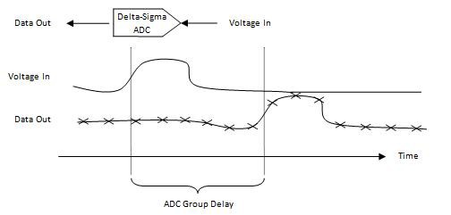
Figure 20. The group delay is the difference between when an input event occurs at the input to the ADC and when the corresponding data is available at the output of the ADC.
The group delay results in a delay between when an input event occurs at the input to the ADC and when the corresponding data is available at the output of the ADC. Put another way, the data returned by the ADC at a given time represents the voltage at the ADC input at some point in the past.
If you do not properly compensate for the group delay, then you get a skew in the data returned by devices with different group delays. In addition, the group delay makes it more difficult to correlate the data returned by these types of ADCs with external events.
Group Delay Compensation
Devices featuring group delay compensation simplify the process of synchronizing between modules and correlating data based on external events. The group delay compensation works via the following mechanisms:
- The sample clock output by these devices is generated at the point in time when the input signal is valid at the ADC input pins. If this sample clock is shared with another device, data from the two devices line up very closely in time regardless of the internal group delay.
- Any triggers generated or received by these devices are interpreted based on their relationships to the generated sample clock. For example, a start trigger that starts an acquisition results in data from the very next sample clock being returned as the first point in the acquisition.
- For any on-demand, software-timed acquisitions, these devices wait for the group delay to elapse before returning a sample from the ADC. As a result, the data returned aligns closely in time with when the data was requested by software.
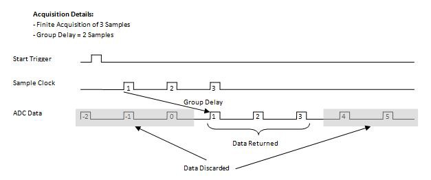
Figure 21. Newer PXI Express devices feature group delay compensation technology that hides the group delay from the end user in most cases.
This acquisition begins with a start trigger from either software or hardware. After receiving the start trigger, the device generates a sample clock as soon as it can. Because the ADC is already running in the background, you must resynchronize the start trigger and align it with the onboard conversions. This process may result in a delay of between zero and two sample clock periods after the start trigger is received before the first sample clock signal is output.
Once sample clock generation begins, it continues based on the number of points desired for this acquisition (three in this example). Internally, the device creates a delayed clock signal used to acquire data from the ADC. This delay value corresponds to the group delay, so the end result is that data returned from the ADC corresponds precisely with the point in time where sample clock edges occurred.
Note that the group delay compensation is performed automatically without users needing to take any special steps in their programs.
Group Delay Compensation Device Support
As of NI-DAQmx 9.1, the NI PXIe-433x bridge input devices support group delay compensation. If you create a multidevice task containing both NI PXIe-433x and PXIe-449x 16-channel DSA modules, NI-DAQmx automatically applies group delay compensation to both devices. However, when used alone, an NI PXIe-449x does not implement group delay compensation.
Group Delay Compensation Caveats
Caveat 1: Latency
Because group delay compensation waits for the desired output data to become available, there is a latency associated with reading the data off these devices.

Figure 22. Because group delay compensation waits for the desired output data to become available, there is a latency associated with reading the data off these devices.
In this example, you start an acquisition and then measure the amount of time that elapses until the first sample becomes available. This delay is equivalent to the group delay of the device at this sample rate. After you get the first sample from the device, the second sample becomes available after only a single sample period’s worth of time elapses. Note that this example ignores software latency as well as any inaccuracy in the software timers used to make this measurement.
Caveat 2: Analog Triggering
These devices include onboard logic to implement an “analog” trigger based on the digitized data returned by the ADC. For this analog trigger to work while still correctly compensating for the group delay of the device, you need to acquire a certain minimum number of pretrigger and posttrigger points.
You do not need to understand exactly how this process works. If you specify an invalid combination of pretrigger and posttrigger samples, then NI-DAQmx provides an error message telling you exactly how to adjust your specified number of samples.
SC Express Flexible Synchronization
The SC Express modules take advantage of the PXI platform and DAQmx driver software to give you many options for synchronizing your hardware. You can chose from sample clock timing and reference clock timing depending on which devices you are using and the level of performance that you require. Though these synchronization methods are highly customizable, NI gives you the option to use multidevice tasks to automatically synchronize modules for you. With the SC Express modules, you can tightly synchronize your hardware and customize to your unique application needs.
